
Datasheet


XC7SET125_1 © NXP B.V. 2009. All rights reserved.
Product data sheet Rev. 01 — 4 September 2009 7 of 14
NXP Semiconductors
XC7SET125
Bus buffer/line driver; 3-state
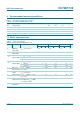
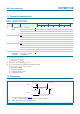
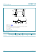
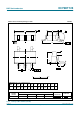
Test data is given in Table 10.
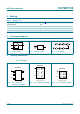
Definitions test circuit:
R
T
= Termination resistance should be equal to output impedance Z
o
of the pulse generator.
C
L
= Load capacitance including jig and probe capacitance.
R
L
= Load resistance.
S1 = Test selection switch.
Fig 9. Test circuit for measuring switching times
V
M
V
M
t
W
t
W
10 %
90 %
0 V
V
I
V
I
negative
pulse
positive
pulse
0 V
V
M
V
M
90 %
10 %
t
f
t
r
t
r
t
f
001aad983
DUT
V
CC
V
CC
V
I
V
O
R
T
R
L
S1
C
L
open
G
Table 10. Test data
Type Input Load S1 position
V
I
t
r
, t
f
C
L
R
L
t
PHL
, t
PLH
t
PZH
, t
PHZ
t
PZL
, t
PLZ
XC7SET125 3 V ≤ 3 ns 15 pF, 50 pF 1 kΩ open GND V
CC