
Datasheet


XC7SH14_1 © NXP B.V. 2009. All rights reserved.
Product data sheet Rev. 01 — 1 September 2009 2 of 14
NXP Semiconductors
XC7SH14
Inverting Schmitt trigger
5. Marking
[1] The pin 1 indicator is located on the lower left corner of the device, below the marking code.
6. Functional diagram
7. Pinning information
7.1 Pinning
7.2 Pin description
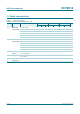
Table 2. Marking codes
Type number Marking code
[1]
XC7SH14GW fF
XC7SH14GV f14
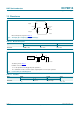
Fig 1. Logic symbol Fig 2. IEC logic symbol Fig 3. Logic diagram
mna023
AY
2
4
24
mna024 mna025
A
Y
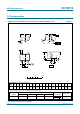
Fig 4. Pin configuration SOT353-1 and SOT753
XC7SH14
n.c. V
CC
A
GND Y
001aak131
1
2
3
5
4
Table 3. Pin description
Symbol Pin Description
n.c. 1 not connected
A 2 data input
GND 3 ground (0 V)
Y 4 data output
V
CC
5 supply voltage