
Datasheet


XC7SH14_1 © NXP B.V. 2009. All rights reserved.
Product data sheet Rev. 01 — 1 September 2009 5 of 14
NXP Semiconductors
XC7SH14
Inverting Schmitt trigger
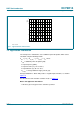
11.1 Transfer characteristics
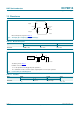
12. Dynamic characteristics
[1] t
pd
is the same as t
PLH
and t
PHL
.
[2] Typical values are measured at V
CC
= 3.3 V.
[3] Typical values are measured at V
CC
= 5.0 V.
[4] C
PD
is used to determine the dynamic power dissipation P
D
(µW).
P
D
=C
PD
× V
CC
2
× f
i
+ ∑(C
L
× V
CC
2
× f
o
) where:
f
i
= input frequency in MHz;
f
o
= output frequency in MHz;
C
L
= output load capacitance in pF;
V
CC
= supply voltage in Volts.
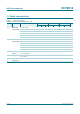
Table 8. Transfer characteristics
At recommended operating conditions; voltages are referenced to GND (ground = 0 V). See Figure 7 and Figure 8.
Symbol Parameter Conditions 25 °C −40 °C to +85 °C −40 °C to +125 °C Unit
Min Typ Max Min Max Min Max
V
T+
positive-going
threshold
voltage
V
CC
= 3.0 V - - 2.2 - 2.2 - 2.2 V
V
CC
= 4.5 V - - 3.15 - 3.15 - 3.15 V
V
CC
= 5.5 V - - 3.85 - 3.85 - 3.85 V
V
T−
negative-going
threshold
voltage
V
CC
= 3.0 V 0.9 - - 0.9 - 0.9 - V
V
CC
= 4.5 V 1.35 - - 1.35 - 1.35 - V
V
CC
= 5.5 V 1.65 - - 1.65 - 1.65 - V
V
H
hysteresis
voltage
V
CC
= 3.0 V 0.3 - 1.2 0.3 1.2 0.25 1.2 V
V
CC
= 4.5 V 0.4 - 1.4 0.4 1.4 0.35 1.4 V
V
CC
= 5.5 V 0.5 - 1.6 0.5 1.6 0.45 1.6 V
Table 9. Dynamic characteristics
GND = 0 V. For waveform see Figure 5. For test circuit see Figure 6.
Symbol Parameter Conditions 25 °C −40 °C to +85 °C −40 °C to +125 °C Unit
Min Typ Max Min Max Min Max
t
pd
propagation
delay
A to Y;
[1]
V
CC
= 3.0 V to 3.6 V
[2]
C
L
= 15 pF - 4.2 12.8 1.0 15.0 1.0 16.5 ns
C
L
= 50 pF - 6.0 16.3 1.0 18.5 1.0 20.5 ns
V
CC
= 4.5 V to 5.5 V
[3]
C
L
= 15 pF - 3.2 8.6 1.0 10.0 1.0 11.0 ns
C
L
= 50 pF - 4.6 10.6 1.0 12.0 1.0 13.5 ns
C
PD
power
dissipation
capacitance
per buffer;
C
L
=50pF;f=1 MHz;
V
I
= GND to V
CC
[4]
-12- - - - - pF