
Datasheet


Analog Integrated Circuit Device Data
12 Freescale Semiconductor
10XSC425
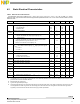
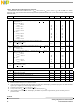
OUTPUTS HS0 TO HS3
R
DS_01(ON)
HS[0,1] Output Drain-to-Source ON Resistance (I
HS
= 5.0 A, T
A
= 25 C)
•V
PWR
= 4.5 V
•V
PWR
= 6.0 V
•V
PWR
= 10 V
•V
PWR
= 13 V
–
–
–
–
–
–
–
–
36
16
10
10
m
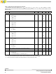
R
DS_01(ON)
HS[0,1] Output Drain-to-Source ON Resistance (I
HS
= 5.0 A, T
A
= 150 C)
•V
PWR
= 4.5 V
•V
PWR
= 6.0 V
•V
PWR
= 10 V
•V
PWR
= 13 V
–
–
–
–
–
–
–
–
62
27
17
17
m
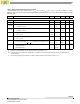
R
SD_01(ON)
HS[0,1] Output Source-to-Drain ON Resistance (I
HS
= -5.0 A, V
PWR=
-18 V)
•T
A
= 25 C
•T
A
= 150 C
–
–
–
–
15
20
m
(13)
R
DS_23(ON)
HS[2,3] Output Drain-to-Source ON Resistance (I
HS
= 5.0 A, T
A
= 25 C)
•V
PWR
= 4.5 V
•V
PWR
= 6.0 V
•V
PWR
= 10 V
•V
PWR
= 13 V
–
–
–
–
–
–
–
–
90
40
25
25
m
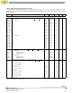
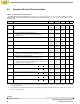
R
DS_23(ON)
HS[2,3] Output Drain-to-Source ON Resistance (I
HS
= 5.0 A, T
A
= 150 C)
•V
PWR
= 4.5 V
•V
PWR
= 6.0 V
•V
PWR
= 10 V
•V
PWR
= 13 V
–
–
–
–
–
–
–
–
153
68
42.5
42.5
m
R
SD_23(ON)
HS[2,3] Output Source-to-Drain ON Resistance (I
HS
= -5.0 A, V
PWR=
-18 V)
•T
A
= 25 C
•T
A
= 150 C
–
–
–
–
37.5
50
m
(13)
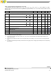
R
SHORT_01
HS[0,1] Maximum Severe Short-circuit Impedance Detection
28 67 100 m
(14)
R
SHORT_23
HS[2,3] Maximum Severe Short-circuit Impedance Detection
70 160 200 m
(14)
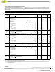
I
OFF
HS[0-3] Output Leakage Current in Off-state
• in sleep mode
• in normal mode (OS_dis = 1 and OLOFF_dis = 1)
–
–
–
–
5.0
30
A
Notes
13. Source-Drain ON Resistance (Reverse Drain-to-Source ON Resistance) with negative polarity V
PWR
.
14. Short-circuit impedance calculated from HS[0:3] to GND pins. Value guaranteed per design.
Table 4. Static Electrical Characteristics (continued)
Characteristics noted under conditions 6.0 V V
PWR
20 V, 3.0 V V
DD
5.5 V, - 40 C T
A
125 C, GND = 0 V, unless
otherwise noted. Typical values noted reflect the approximate parameter means at T
A
= 25 °C under nominal conditions, unless
otherwise noted.
Symbol Characteristic Min Typ Max Unit Notes