
Datasheet


September 1993 2
Philips Semiconductors Product specification
Octal D-type transparent latch; 3-state 74HC/HCT373
FEATURES
• 3-state non-inverting outputs for bus oriented
applications
• Common 3-state output enable input
• Functionally identical to the “563”, “573” and “533”
• Output capability: bus driver
• I
CC
category: MSI
GENERAL DESCRIPTION
The 74HC/HCT373 are high-speed Si-gate CMOS devices
and are pin compatible with low power Schottky TTL
(LSTTL). They are specified in compliance with JEDEC
standard no. 7A.
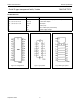
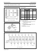
The 74HC/HCT373 are octal D-type transparent latches
featuring separate D-type inputs for each latch and 3-state
outputs for bus oriented applications. A latch enable (LE)
input and an output enable (
OE) input are common to all
latches.
The “373” consists of eight D-type transparent latches with
3-state true outputs. When LE is HIGH, data at the D
n
inputs enters the latches. In this condition the latches are
transparent, i.e. a latch output will change state each time
its corresponding D-input changes.
When LE is LOW the latches store the information that was
present at the D-inputs a set-up time preceding the
HIGH-to-LOW transition of LE. When OE is LOW, the
contents of the 8 latches are available at the outputs.
When OE is HIGH, the outputs go to the high impedance
OFF-state. Operation of the OE input does not affect the
state of the latches.
The “373” is functionally identical to the “533”, “563” and
“573”, but the “563” and “533” have inverted outputs and
the “563” and “573” have a different pin arrangement.
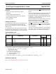
QUICK REFERENCE DATA
GND = 0 V; T
amb
=25°C; t
r
=t
f
= 6 ns
Notes
1. C
PD
is used to determine the dynamic power dissipation (P
D
in µW):
P
D
=C
PD
× V
CC
2
× f
i
+∑ (C
L
× V
CC
2
× f
o
) where:
f
i
= input frequency in MHz
f
o
= output frequency in MHz
∑ (C
L
× V
CC
2
× f
o
) = sum of outputs
C
L
= output load capacitance in pF
V
CC
= supply voltage in V
2. For HC the condition is V
I
= GND to V
CC
. For HCT the condition is V
I
= GND to V
CC
− 1.5 V
ORDERING INFORMATION
See
“74HC/HCT/HCU/HCMOS Logic Package Information”
.
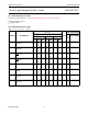
SYMBOL PARAMETER CONDITIONS
TYPICAL
UNIT
HC HCT
t
PHL
/ t
PLH
propagation delay C
L
= 15 pF; V
CC
=5V
D
n
to Q
n
12 14 ns
LE to Q
n
15 13 ns
C
I
input capacitance 3.5 3.5 pF
C
PD
power dissipation capacitance per latch notes 1 and 2 45 41 pF