
Datasheet


BGA7130 All information provided in this document is subject to legal disclaimers. © NXP B.V. 2012. All rights reserved.
Product data sheet Rev. 1 — 9 October 2012 4 of 27
NXP Semiconductors
BGA7130
400 MHz to 2700 MHz 1 W high linearity silicon amplifier
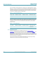
8. Pinning information
8.1 Pinning
8.2 Pin description
[1] This pin can be connected to ground.
[2] This pin requires an external DC-blocking capacitor.
[3] RF decoupled.
[4] The exposed die pad of the SOT908-3 also functions as heatsink for the power amplifier.
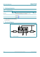
Fig 2. Pin configuration
(1$%/(
5)B287
5)B287
5)B,1
QF
7UDQVSDUHQWWRSYLHZ
,&4B$'-
WHUPLQDO
LQGH[DUHD
%*$
QF
DDD
9
&&
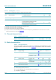
Table 4. Pin description
Symbol Pin Description
n.c. 1, 4 not connected
[1]
RF_OUT 2, 3 RF output and supply to the amplifier
[2]
V
CC
5 bias supply voltage
[3]
ENABLE 6 enable
RF_IN 7 RF input
[2]
ICQ_ADJ 8 quiescent collector current adjustment by an external resistor
GND exposed die pad ground
[4]