
Datasheet


BGA7130 All information provided in this document is subject to legal disclaimers. © NXP B.V. 2012. All rights reserved.
Product data sheet Rev. 1 — 9 October 2012 5 of 27
NXP Semiconductors
BGA7130
400 MHz to 2700 MHz 1 W high linearity silicon amplifier
9. Functional description
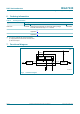
9.1 Supply current adjustment
The supply current can be adjusted by changing the value of biasing resistor R3 which
connects pin ICQ_ADJ (pin 8) to ground (see Figure 1
).
9.2 Enable control
The BGA7130 can be powered down using enable pin 6 (ENABLE). In case this control
function is not needed the enable pin can be connected to the bias supply voltage pin 5
(V
CC
). The current through the enable pin 6 should never exceed 20 mA as this might
damage the ESD protection circuitry. This can be avoided either by preventing the voltage
on this pin to exceed the supply voltage (V
SUP
) or by adding a series resistor.
10. Limiting values
V
SUP
= 5 V; T
amb
= 25 C.
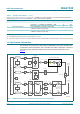
Fig 3. Supply current I
CC(tot)
as function of biasing resistor R3; typical values
DDD
5ȍ
,
&&WRW&&WRW
,
&&WRW
P$P$P$
Table 5. Enable truth table
Logic level on pin ENABLE (pin 6) Status BGA7130
LOW powered down
HIGH powered on
Table 6. Limiting values
In accordance with the Absolute Maximum Rating System (IEC 60134).
Symbol Parameter Conditions Min Max Unit
V
SUP
supply voltage
[1]
0.5 +7 V
V
I(dig)
digital input voltage
[2][4]
0V
SUP
V
I
I(dig)
digital input current
[3][4]
20 +20 mA
I
CC(tot)
total supply current - 1000 mA