
Datasheet


BGA7130 All information provided in this document is subject to legal disclaimers. © NXP B.V. 2012. All rights reserved.
Product data sheet Rev. 1 — 9 October 2012 6 of 27
NXP Semiconductors
BGA7130
400 MHz to 2700 MHz 1 W high linearity silicon amplifier
[1] Absolute maximum DC voltage on pins RF_OUT, ICQ_ADJ and V
CC
.
[2] Absolute maximum DC voltage on pin ENABLE.
[3] Absolute maximum DC current through pin ENABLE.
[4] If V
I(dig)
exceeds V
SUP
the internal ESD protection circuit can be damaged. The pin ENABLE can be connected to V
CC
in case the
enable control function is not used (see Section 9.2
).
11. Thermal characteristics
12. Static characteristics
[1] Supply voltage on pins RF_OUT and V
CC
.
[2] Current through pins RF_OUT and V
CC
.
[3] T
case
is the temperature at the soldering point of the exposed die pad.
[4] On digital input pin ENABLE.
P
i(RF)
RF input power f = 750 MHz; switched - 18 dBm
f = 2140 MHz; switched - 25 dBm
T
stg
storage temperature 65 +150 C
T
j
junction temperature - 150 C
V
ESD
electrostatic discharge voltage Human Body Model (HBM);
According JEDEC standard 22-A114E
-6 kV
Charged Device Model (CDM);
According JEDEC standard 22-C101B
-2 kV
Table 6. Limiting values
…continued
In accordance with the Absolute Maximum Rating System (IEC 60134).
Symbol Parameter Conditions Min Max Unit
Table 7. Thermal characteristics
Symbol Parameter Conditions Typ Unit
R
th(j-case)
thermal resistance from junction to case T
case
<85C6K/W
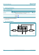
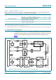
Table 8. Static characteristics
4.75 V
V
SUP
5.25 V;
40
C
T
case
+85
C; P
i
<
20 dBm; R3 = 523
(tolerance 1 %); input
and output impedances matched to 50
(see Section 14); pin ENABLE = HIGH; unless otherwise
specified.
Symbol Parameter Conditions Min Typ Max Unit
V
SUP
supply voltage
[1]
4.75 - 5.25 V
I
CC(tot)
total supply current
[2]
390 450 510 mA
0 R3 5k
[2]
30 - 550 mA
0 R3 5k;
pin ENABLE = LOW
[2]
-4 6 A
T
case
case temperature
[3]
40 +25 +85 C
I
CC
supply current on pin RF_OUT - 420 - mA
on pin V
CC
-30- mA
on pin ENABLE - - 3 A
V
IL
LOW-level input voltage
[4]
0- 0.7V
V
IH
HIGH-level input voltage
[4]
2.5 - V
SUP
V