
Datasheet


BGA7130 All information provided in this document is subject to legal disclaimers. © NXP B.V. 2012. All rights reserved.
Product data sheet Rev. 1 — 9 October 2012 7 of 27
NXP Semiconductors
BGA7130
400 MHz to 2700 MHz 1 W high linearity silicon amplifier
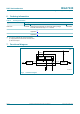
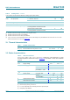
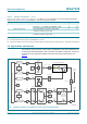
13. Dynamic characteristics
Table 9. Dynamic characteristics
4.75 V
V
SUP
5.25 V;
40
C
T
case
85
C; P
i
<
20 dBm; R3 = 523
(tolerance 1 %); input and output impedances
matched to 50
(see Section 14); pin ENABLE = HIGH; unless otherwise specified.
Symbol Parameter Conditions Min Typ Max Unit
f frequency 400 - 2700 MHz
Measured at LTE-750 MHz (see Section 14
)
f frequency
[1]
728 748 768 MHz
G
p
power gain 728 MHz f 768MHz 172023dB
728 MHz f 768 MHz; pin ENABLE = LOW - 18 - dB
P
L(1dB)
output power at 1 dB gain
compression
728 MHz f 768 MHz 27 30.5 - dBm
IP3
O
output third-order intercept point 728 MHz f 768 MHz; P
L
= 15 dBm per tone;
tone spacing = 1 MHz
39 42.5 - dBm
EVM error vector magnitude E-UTRA Test Model (E-TM) 3.1 LTE;
P
L(AV)
=20dBm
-2-%
NF noise figure 728 MHz f 768 MHz - 5 - dB
RL
in
input return loss 728 MHz f 768 MHz - 6 - dB
728 MHz f 768 MHz; pin ENABLE = LOW - 1 - dB
RL
out
output return loss 728 MHz f 768 MHz - 10 - dB
728 MHz f 768 MHz; pin ENABLE = LOW - 0.5 - dB
ISL isolation 728 MHz f 768 MHz - 29 - dB
728 MHz f 768 MHz; pin ENABLE = LOW - 18 - dB
t
d(pu)
power-up delay time after pin ENABLE is switched to logic HIGH;
to within 0.1 dB of final gain state.
-3-s
t
d(pd)
power-down delay time after pin ENABLE is switched to logic LOW;
to within 0.1 dB of final gain state.
-0.5-s
Measured at UMTS-2140 MHz (see Section 14
)
f frequency
[2]
2110 2140 2170 MHz
G
p
power gain 2110 MHz f 2170 MHz 9 12 15 dB
2110 MHz f 2170 MHz; pin ENABLE = LOW - 15 - dB
P
L(1dB)
output power at 1 dB gain
compression
2110 MHz f 2170 MHz 27 30 - dBm
IP3
O
output third-order intercept point 2110 MHz f 2170 MHz;
P
L
= 15 dBm per tone; tone spacing = 1 MHz
41 44 - dBm
ACPR adjacent channel power ratio 2110 MHz f 2170 MHz
[3]
- 60 - dBc
NF noise figure 2110 MHz f 2170 MHz - 5 - dB
RL
in
input return loss 2110 MHz f 2170 MHz - 6 - dB
2110 MHz f 2170 MHz; pin ENABLE = LOW - 3 - dB
RL
out
output return loss 2110 MHz f 2170 MHz - 10 - dB
2110 MHz f 2170 MHz; pin ENABLE = LOW - 1 - dB