
Datasheet


BGA7130 All information provided in this document is subject to legal disclaimers. © NXP B.V. 2012. All rights reserved.
Product data sheet Rev. 1 — 9 October 2012 8 of 27
NXP Semiconductors
BGA7130
400 MHz to 2700 MHz 1 W high linearity silicon amplifier
[1] Covering downlink frequency range of eUTRAN bands 11, 13, 14 and 17.
[2] Covering downlink frequency range of eUTRAN bands 1, 4 and 10.
[3] Two carrier W-CDMA; each carrier according to 3GPP test model 1; 64 DPCH; PAR for composite signal = 7 dB; 5 MHz carrier spacing.
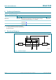
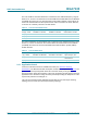
14. Application information
The BGA7130 can be used for a wide variety of applications. This section describes two
example base station applications: LTE at 750 MHz and UMTS at 2140 MHz. It serves as
a pre-driver for the high-power amplifier in the Base Transceiver Station (BTS), see
Figure 4
.
ISL isolation 2110 MHz f 2170 MHz - 24 - dB
2110 MHz f 2170 MHz; pin ENABLE = LOW - 15 - dB
t
d(pu)
power-up delay time after pin ENABLE is switched to logic HIGH;
to within 0.1 dB of final gain state.
-3-s
t
d(pd)
power-down delay time after pin ENABLE is switched to logic LOW;
to within 0.1 dB of final gain state.
-0.5-s
Table 9. Dynamic characteristics …continued
4.75 V
V
SUP
5.25 V;
40
C
T
case
85
C; P
i
<
20 dBm; R3 = 523
(tolerance 1 %); input and output impedances
matched to 50
(see Section 14); pin ENABLE = HIGH; unless otherwise specified.
Symbol Parameter Conditions Min Typ Max Unit
Fig 4. Simplified schematic representation of a Base Transceiver Station (BTS)
DDD
6(5,'$&
/3)
/3)
,)PL[HU
,402'
%3)
7;%3)
DWWHQXDWRU
&/2&.
3//
9&2
9*$
9*$
5;%3)
5;%3)
9*$ +3$
/1$
%*$
/1$
&
&
/1$
GXSOH[HU
DQWHQQD
7;5;
DQWHQQD
5;
LVRODWRU
3//
9&2
6(54'$&
6(5'$&
/3)
/3)
/1$
&/2&.
6(5'$&
6(5$'&
32:(5$03/,),(5
',*,7$/%$6(%$1'$1'&21752/
PL[HU
PL[HU
PL[HU
,)PL[HU
3//
9&2
72:(5
02817('
$03/,),(5
PL[HU
PL[HU