
Datasheet


FEATURES
Operating Characteristics
} Voltage range: 2.7 to 5.5 V
} Flash write voltage range: 2.7 to 5.5 V
} Temperature range (ambient): –40 °C
to +105 °C
Performance
} Up to 48 MHz ARM Cortex-M0+ core
} Single-cycle 32-bit x 32-bit multiplier
} Single-cycle I/O access port
Memories and Memory Interfaces
} Up to 128 KB flash
} Up to 16 KB RAM
} Up to 256 B EEPROM
Clocks
} Oscillator (XOSC): Loop-controlled
Pierce oscillator, crystal or ceramic
resonator range of 31.25 to 39.0625
kHz or 4 to 20 MHz
} Internal clock source (ICS): Internal FLL
with internal or external reference,
precision trimming of internal
reference allowing 1% deviation across
temperature range of 0 °C to 70 °C and
1.5% deviation across temperature range
of –40 °C to +105 °C, up to 48 MHz
} Internal 1 kHz low-power oscillator (LPO)
System Peripherals
} Power management module (PMC) with
three power modes: run, wait and stop
} Low-voltage detection (LVD) with reset
or interrupt, selectable trip points
} Watchdog with independent clock
source (WDOG)
} Programmable cyclic redundancy
check module (CRC)
} Serial wire debug interface (SWD)
} Bit manipulation engine (BME)
} Security and Integrity Modules
} 64-bit unique identification (ID)
number per chip
Human-Machine Interface
} Up to 71 general-purpose input/
output (GPIO)
} Two 8-bit keyboard interrupt
modules (KBI)
} Up to 8 ultra-high-current sink pins
supporting 20 mA source/sink current
Analog Modules
} One 16-channel 12-bit SAR ADC with
internal band gap reference channel,
operation in stop mode, optional
hardware trigger (ADC)
} Two analog comparators containing
a 6-bit DAC and programmable
reference input (ACMP)
Timers
} One 6-channel FlexTimer/PWM (FTM)
} Two 2-channel FlexTimer/PWM (FTM)
} One 2-channel periodic interrupt
timer (PIT)
} One real-time clock (RTC)
} One pulse width timer (PWT)
} Serial Interfaces
} Three UART Interfaces (LIN capable)
} Two Serial Peripheral Interfaces
} Two I2C interfaces
} One CAN module
TOOLS
Freedom Development
Platforms Features:
} Capacitive touch slider, MMA8451Q
accelerometer, Tri-color LED
} Flexible power supply options—USB
and external source
} Easy access to MCU I/O
} IrDA transmitter and receiver
} Thermistor sensor to measuring
temperature
} Form factor compatible with Arduino
™
R3 pin layout
} New, OpenSDA debug interface
– Mass storage device flash
programming interface (default)
– Tool installation not required to
evaluate demo apps
– P&E Microcomputer Systems
®
Debug interface provides run-control
debugging and compatibility with
IDE tools
– CMSIS-DAP interface: new ARM
standard for embedded
Learn more at: www.nxp.com/freedom
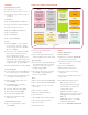
64-bit unique
identification (ID)
number
Watchdog
Low-voltage
detection
Cyclic redundancy
check
Serial wire debug
Bit manipulation
engine
Power management
module
Kinetis KE0x Block Diagram
HMI Memory Interfaces
System Core Complex Analog
Clocks
Security Communications
Timers
Up to 2 x SPI
Up to 2 x I
2
C
Up to 1 CAN
Up to 3 x UART
Up to 128 KB Flash
Up to 16 KB RAM
256 B EEPROM
Internal oscillator
Internal reference
clocks
Frequency locked
loop
One six-channel
FlexTimer/PWM
One Pulse
Width Timer
One two-channel
periodic
interrupt timer
RTC
ARM
®
Cortex
®
-M0+
Up to 48 MHz
Single-cycle I/O
access port
Single-cycle
32-bit x 32-bit
multiplier
Up to 71 GPIO
1 x 12-bit ADC
2 x analog
comparator
2 x KBI
Up to 8 high-
current pins (20mA)
Up to Two two-channel
FlexTimer/PWM
Proprietary TechnologyOptional
KINETIS KE0x FAMILY BLOCK DIAGRAM