
Datasheet


NXP Semiconductors
MF0ICU2
MIFARE Ultralight C - Contactless ticket IC
MF0ICU2 All information provided in this document is subject to legal disclaimers. © NXP B.V. 2019. All rights reserved.
Product data sheet Rev. 3.3 — 30 July 2019
COMPANY PUBLIC 137633 14 / 36
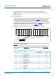
# PCD Data exchanged PICC
2 ←
AF577293FD2F34CA51
generate RndB = 51E764602678DF2B
IV = 0000000000000000
ek(RndB) = 577293FD2F34CA51
3 decipher ek(RndB) to retrieve RndB
generate RndA = A8AF3B256C75ED40
RndB’ = E764602678DF2B51
RndA+RndB’ =
A8AF3B256C75ED40E764602678DF2B51
IV = 577293FD2F34CA51
ek(RndA+RndB´) =
0A638559FC7737F9F15D7862EBBE967A
→
AF0A638559FC7737F9
F15D7862EBBE967A
4 ←
003B884FA07C137CE1
decipher ek(RndA+RndB´) to retrieve RndA
verify RndB’
RndA’=AF3B256C75ED40A8
IV = F15D7862EBBE967A
ek(RndA´)= 3B884FA07C137CE1
5 decipher and verify ek(RndA’)
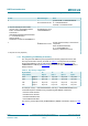
7.5.7 Programming of 3DES key to memory
The 16 bytes of the 3DES key are programmed to memory pages from 2Ch to 2Fh.
The keys are stored in memory as shown in Table 10. The key itself can be written
during personalization or at any later stage using the WRITE (see Section 9.3) or
COMPATIBILITY WRITE (see Section 9.4) command. For both commands, Byte 0 is
always sent first.
Table 10. Key memory configuration
Byte address 0h 1h 2h 3h
Page address Byte 0 Byte 1 Byte 2 Byte 3
2Ch Page 44 Key1 / K0 Key1 / K1 Key1 / K2 Key1 / K3
2Dh Page 45 Key1 / K4 Key1 / K5 Key1 / K6 Key1 / K7
2Eh Page 46 Key2 / K0 Key2 / K1 Key2 / K2 Key2 / K3
2Fh Page 47 Key2 / K4 Key2 / K5 Key2 / K6 Key2 / K7
On example of Key1 = 0001020304050607h and Key2 = 08090A0B0C0D0E0Fh, the
command sequence needed for key programming with WRITE command is:
• A2 2C 07 06 05 04 CRC
• A2 2D 03 02 01 00 CRC
• A2 2E 0F 0E 0D 0C CRC
• A2 2F 0B 0A 09 08 CRC
The memory content after those (COMPATIBILITY) WRITE commands is shown in Table
11.