
Datasheet


NXP Semiconductors
MF0ICU2
MIFARE Ultralight C - Contactless ticket IC
MF0ICU2 All information provided in this document is subject to legal disclaimers. © NXP B.V. 2019. All rights reserved.
Product data sheet Rev. 3.3 — 30 July 2019
COMPANY PUBLIC 137633 26 / 36
treatment ground and stress relieve
R
a
max = 0.2 μmroughness
R
t
max = 2 μm
Chip dimensions
x = 710 μmstep size
[1]
y = 710 μm
typical = 22 μmgap between chips
[1]
minimum = 5 μm
Passivation
type sandwich structure
material PSG / nitride
thickness 500 nm / 600 nm
Au bump (substrate connected to VSS)
material > 99.9 % pure Au
hardness 35 to 80 HV 0.005
shear strength > 70 MPa
height 18 μm
within a die = ±2 μm
within a wafer = ±3 μm
height uniformity
wafer to wafer = ±4 μm
flatness minimum = ±1.5 μm
size LA, LB, VSS, TP1, TP2
[2]
= 60 μm × 60 μm
size variation ±5 μm
under bump metallization sputtered TiW
[1] The step size and the gap between chips may vary due to changing foil expansion
[2] Pads VSS and TESTIO are disconnected when wafer is sawn.
12.1 Fail die identification
Electronic wafer mapping covers the electrical test results and additionally the results of
mechanical/visual inspection. No ink dots are applied.
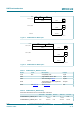
12.2 Package outline
For more details on the contactless modules MOA4 and MOA8 please refer to Ref. 11
and Ref. 12.