
Datasheet


NXP Semiconductors
MF0ICU2
MIFARE Ultralight C - Contactless ticket IC
MF0ICU2 All information provided in this document is subject to legal disclaimers. © NXP B.V. 2019. All rights reserved.
Product data sheet Rev. 3.3 — 30 July 2019
COMPANY PUBLIC 137633 5 / 36
7 Functional description
7.1 Block description
The MF0ICU2 chip consists of a 1536-bit EEPROM, an RF-Interface and the Digital
Control Unit. Energy and data are transferred via an antenna, which consists of a coil
with a few turns directly connected to the MF0ICU2. No further external components are
necessary. For details on antenna design please refer to the document Ref. 7.
• RF-Interface:
– Modulator/Demodulator
– Rectifier
– Clock Regenerator
– Power On Reset
– Voltage Regulator
• Crypto coprocessor: Triple - Data Encryption Standard (3DES) coprocessor
• Crypto control unit: controls Crypto coprocessor operations
• Command Interpreter: Handles the commands supported by the MF0ICU2 in order to
access the memory
• EEPROM-Interface
• EEPROM: The 1536 bits are organized in 48 pages with 32 bits each. 80 bits are
reserved for manufacturer data. 32 bits are used for the read-only locking mechanism.
32 bits are available as OTP area. 1152 bits are user programmable read/write
memory.
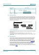
7.2 State diagram and logical states description
The commands are initiated by the PCD and controlled by the Command Interpreter of
the MF0ICU2. It handles the internal states (as shown in Figure 4) and generates the
appropriate response.
For a correct implementation of an anticollision procedure please refer to the documents
in Section 14.