
Datasheet


NXP Semiconductors
MF0ICU2
MIFARE Ultralight C - Contactless ticket IC
MF0ICU2 All information provided in this document is subject to legal disclaimers. © NXP B.V. 2019. All rights reserved.
Product data sheet Rev. 3.3 — 30 July 2019
COMPANY PUBLIC 137633 8 / 36
state via the HLTA command. This state helps the PCD to distinguish between already
processed cards and cards that have not been selected yet. The only way to get the
MF0ICU2 out of this state is the WUPA command or a RF reset. Any other data received
in this state is interpreted as an error and the MF0ICU2 remains in this state.
7.2.6 AUTHENTICATED
In the AUTHENTICATED state either a READ or a WRITE command may be performed
to memory areas, which are only readable and/or writeable after authentication.
Authentication is performed using the 3DES Authentication described in Section 7.5.5.
7.3 Data integrity
The following mechanisms are implemented in the contactless communication link
between PCD and MF0ICU2 to ensure a reliable data transmission:
• 16 bits CRC per block
• Parity bit for each byte
• Bit count checking
• Bit coding to distinguish between "1", "0", and no information
• Channel monitoring (protocol sequence and bit stream analysis)
7.4 RF interface
The RF-interface is implemented according to the standard for contactless smart cards
ISO/IEC 14443 Type A (see Ref. 1 and Ref. 2).
The RF-field from the PCD is always present (with short modulation pulses when
transmitting), because it is used for the power supply of the card.
For both directions of data communication there is one start bit at the beginning of each
frame. Each byte is transmitted with a parity bit (odd parity) at the end. The LSBit of the
byte with the lowest byte address within selected page is transmitted first. The maximum
frame length is 164 bits (16 data bytes + 2 CRC bytes = 16 * 9 + 2 * 9 + 1 start bit + 1
end bit).
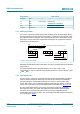
7.5 Memory organization
The 1536-bit EEPROM memory is organized in 48 pages with 32 bits each. In the erased
state the EEPROM cells are read as a logical "0", in the written state as a logical "1".
Table 5. Memory organization
Page address Byte number
Decimal Hex 0 1 2 3
0 00h serial number
1 01h serial number
2 02h serial number internal lock bytes lock bytes
3 03h OTP OTP OTP OTP
4 to 39 04h to 27h user memory user memory user memory user memory
40 28h lock bytes lock bytes - -