
Datasheet


Philips Semiconductors Product specification
82B715I
2
C bus extender
2001 Mar 06
5
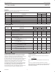
RATINGS
Limiting values in accordance with the Absolute Maximum System (IEC 134).
Voltages with respect to pin GND (DIL-8 pin 4).
LIMITS
SYMBOL PARAMETER MIN. MAX. UNIT
V
CC
to GND Supply voltage range V
CC
–0.3 +12 V
V
bus
Voltage range I
2
C Bus, SCL or SDA 0 V
CC
V
V
buff
Voltage range Buffered Bus 0 V
CC
V
I DC current (any pin) 60 mA
P
tot
Power dissipation 300 mW
T
stg
Storage temperature range –55 +125 °C
T
amb
Operating ambient temperature range –40 +85 °C
CHARACTERISTICS
At T
amb
= +25°C and V
CC
= 5 Volts, unless otherwise specified.
LIMITS
SYMBOL PARAMETER MIN. TYP. MAX. UNIT
Power Supply
V
CC
Supply voltage (operating) 4.5 — 12 V
I
CC
Supply current — 16 — mA
I
CC
Supply current at V
CC
= 12V — 22 — mA
I
CC
Supply current, both I
2
C inputs LOW,
both buffered outputs sinking 30mA.
— 28 — mA
Drive Currents
I
Sx
, I
Sy
Output sink on I
2
C bus
V
Sx
, V
Sy
LOW = 0.4V
V
Lx
, V
Ly
LOW on Buffered bus = 0.3V
3 — — mA
I
Lx
, I
Ly
Output sink on Buffered bus
V
Lx
, V
Ly
LOW = 0.4V
V
Sx
, V
Sy
LOW on I
2
C bus = 0.3V
30 — — mA
Input Currents
I
Sx
, I
Sy
Input current from I
2
C bus when
I
Lx
, I
Ly
sink on Buffered bus = 30mA
— — 3 mA
I
Lx
, I
Ly
Input current from Buffered bus when
I
Sx
, I
Sy
sink on I
2
C bus = 3mA
— — 3 mA
I
Lx
, I
Ly
Leakage current on Buffered bus
V
Lx
, V
Ly
= V
CC
, and V
Sx
, V
Sy
= V
CC
— — 200 µA
Impedance Transformation
Z
in
/Z
out
Input/Output impedance 8 10 13
Pull-Up Resistance Calculation
In calculating the pull-up resistance values, the gain of the buffer
introduces scaling factors which must be applied to the system
components. Viewing the system from the Buffered bus, all I
2
C bus
capacitances have effectively 10 times their I
2
C bus value.
In practical systems the pull-up resistance is determined by the rise
time limit for I
2
C systems. As an approximation this limit will be
satisfied if the time constant (product of the net resistance and net
capacitance) of the total system is set to 1 microsecond.
The total time constant may either be set by considering each bus
node individually (i.e., the I
2
C nodes, and the Buffered bus node)
and choosing pull-up resistors to give time constants of 1
microsecond for each node; or by combining the capacitances into
an equivalent capacitive loading on the Buffered bus, and
calculating the Buffered bus pull-up resistor required by this
equivalent capacitance.
For each separate bus the pull-up resistor may be calculated as
follows:
R +
1m sec
C
device
) C
wiring
Where: C
device
= sum of device capacitances connected to each
bus,
and C
wiring
= total wiring and stray capacitance on each bus.
If these capacitances are not known then a good approximation is to
assume that each device presents 10pF of load capacitance and
10pF of wiring capacitance.