
Datasheet


May 1992 7
Philips Semiconductors Product specification
2 x 22 W or 4 x 11 W single-ended car
radio power amplifier
TDA1558Q
Notes to the characteristics
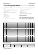
1. All characteristics are measured using the circuit shown in Fig.4
2. The circuit is DC adjusted at V
P
= 6 to 18 V and AC operating at V
P
= 8.5 to 18 V.
3. At 18 V < V
P
< 30 V, the DC output voltage ≤ V
P
/2.
4. Frequency response externally fixed.
5. Ripple rejection measured at the output with a source-impedance of 0 Ω (max. ripple amplitude of 2 V) and a
frequency between 100 Hz and 10 kHz.
6. Noise voltage measured in a bandwidth of 20 Hz to 20 kHz.
7. Noise output voltage independent of R
S
(V
in
= 0).
8. Output power is measured directly at the output pins of the IC.
|Z
I
| input impedance 25 30 38 kΩ
V
no
noise output voltage
ON; R
S
= 0; note 6 − 200 300 µV
R
S
= 10 kΩ; note 6 − 350 −µV
MUTE; notes 6 and 7 − 180 −µV
α channel separation R
S
= 10 kΩ 40 −−dB
|∆G
v
| channel unbalance −− 1dB
Quad single-ended application (see Fig.5)
P
O
output power note 8
THD = 0.5% 4 5 − W
THD = 10% 5.5 6 − W
R
L
= 2 Ω; THD = 0.5% 7.5 8.5 − W
R
L
= 2 Ω; THD = 10% 10 11 − W
THD total harmonic distortion P
O
= 1 W − 0.1 − %
f
low
low frequency roll-off −3 dB; note 4 − 45 − Hz
f
high
high frequency roll-off −1 dB 20 −−kHz
G
v
closed loop voltage gain 39 40 41 dB
SVRR supply voltage ripple rejection note 5
ON 44 −−dB
MUTE 44 −−dB
stand-by 80 −−dB
|Z
I
| input impedance 50 60 75 kΩ
V
no
noise output voltage
ON; R
S
= 0; note 6 − 150 230 µV
R
S
= 10 kΩ; note 6 − 250 −µV
MUTE; notes 6 and 7 − 120 −µV
α channel separation R
S
= 10 kΩ 40 −−dB
|∆G
v
| channel unbalance −− 1dB
SYMBOL PARAMETER CONDITIONS MIN. TYP. MAX. UNIT