
Datasheet


2003 Oct 14 11
Philips Semiconductors Product specification
High speed CAN transceiver TJA1040
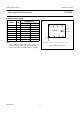
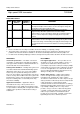
BONDING PAD LOCATIONS
Note
1. All x/y coordinates represent the position of the centre
of each pad (in µm) with respect to the left hand
bottom corner of the top aluminium layer (see Fig.9).
SYMBOL PAD
COORDINATES
(1)
xy
TXD 1 119.5 114.5
GND 2 648.5 85
V
CC
3 1214.25 114.5
RXD 4 1635.25 114.5
SPLIT 5 1516.5 1275
CANL 6 990.5 1273.75
CANH 7 530.25 1273.75
STB 8 113.75 1246
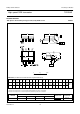
handbook, halfpage
MBL584
8
TJA1040U
76 5
1
234
y
x
0
0
test pad 1
test pad 2
Fig.9 Bonding pad locations.
The backside of the bare die must be connected to ground.