
Daim Ntawv Qhia Tus Neeg Siv
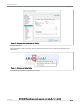
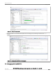
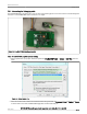
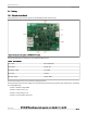
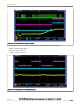
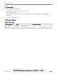
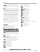

Table Of Contents

7.4 Testing
7.4.1 Signals on the Board
The following figure shows the main signals on the WPR1500-HV EPP receiver board.
Figure 18. Important test points on WPR1500-HV board
The following table lists the testing points on the WPR1500 BUCK board.
Table 3. Test Points list
TP1 : VDD TP9: CLAMP_EN
TP2 : TEST J2 & J4: I2C
TP3 & TP4 : ACIN J3: V_REC
TP5 : IOUT J6: CTX
TP7 & J7: VOUT J5 & J8: GND
The following examples show how to measure and debug the board.
The following figure shows the input voltage and communication signal from the ping phase to power transfer setup. The loading
is 10.5W(12V@0.875A)
• Channel 1: Rectifier voltage VREC
• Channel 2: Output current I_out
• Channel 3: Output voltage V_out
• Channel 4: Communication signal CTX
NXP Semiconductors
Getting Started
WPR1500-HV Wireless Charging Receiver Application User’s Guide, Rev. 3.0, 4 July 2022
User Guide 12 / 17