
User manual
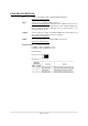


INPUT/OUTPUT:
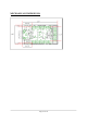
User button with name BUT – connected to STM32F103RBT6 pin.14 PA0.WKUP;
Status green LED with name STAT connected to STM32F103RBT6 pin.53 PC12, note that
LED-E SMT jumper should be shorted to may LED work properly (it’s shorted by default),
if you decide to use PC12 port for other purpose you have to remove the solder short on this
jumper which will disconnect the LED from PC12 port;
Power supply red LED with name PWR – indicates that 3.3V power supply is applied;
JTAG:
The JTAG connector allows the software debugger to talk via a JTAG (Joint
Test Action Group) port directly to the core. Instructions may be inserted and
executed by the core thus allowing STM32F103RBT6 memory to be
programmed with code and executed step by step by the host software.
For more details refer to IEEE Standard 1149.1 - 1990 Standard Test Access
Port and Boundary Scan Architecture and STM32F103RBT6 datasheets and
users manual.
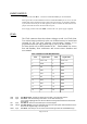
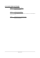
JTAG CONNECTOR PIN DESCRIPTIONS
Pin # Signal Name Pin # Signal Name
1 TVCC 3.3V 2 TVCC 3.3V
3 TRST 4 GND
5 TDI 6 GND
7 TMS 8 GND
9 TCK 10 GND
11 NC 12 GND
13 TDO 14 GND
15 RST 16 GND
17 NC 18 GND
19 NC 20 GND
TMS Input Test Mode Select. The TMS pin selects the next state in the TAP state machine.
TCK Input Test Clock. This allows shifting of the data in, on the TMS and TDI pins.
It is a positive edgetriggered clock with the TMS and TCK signals that define the internal state
of the device.
TDI Input Test Data In. This is the serial data input for the shift register.
TDO Output Test Data Output. This is the serial data output from the shift register. Data is shifted out of the
device on the negative edge of the TCK signal.
TRST Input Test Reset. The TRST pin can be used to reset the test logic within the EmbeddedICE logic.
Page 12 of 18