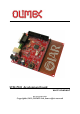
STM-P103 development board user's manual Rev.
INTRODUCTION: STM32-P103 board is development board which allow exploring the complete features of the new ARM Cortex M3 STM32F103RBT6 microcontrollers produced by ST Microelectronics Inc. The board have SD/MMC card connector and allow USB Mass storage device demo to be evaluated. The RS232 driver and connector allow USB to Virtual COM port demo to be evaluated. The CAN port and driver allow CAN applications to be developed.
BOARD USE REQUIREMENTS: Cables: 1.8 meter USB A-B cable to connect to USB host. Hardware: ARM-JTAG, ARM-USB-OCD, ARM-USB-TINY or other ARM JTAG compatible tool Software: ARM C compiler and debugger software, the possible options are: - free open source platform: GNU C compiler + OpenOCD and Eclipse (support all low cost Olimex JTAG debuggers) - commercial solution EW-ARM from IAR Systems AB, require expensive J-LINK debugger - CrossWorks from Rowley (supports all Olimex low cost JTAG debuggers).
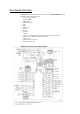
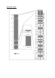
SCHEMATIC:
PROCESSOR FEATURES: STM-P103 board use ARM 32-bit Cortex™-M3 CPU STM32F103RBT6 from ST Microelectronics with these features: - CPU clock up to 72Mhz - FLASH 128KB - RAM 20KB - DMA x7 channels - RTC - WDT - Timers x3+1 - SPI x2 - I2C x2 - USART x3 - USB x1 - CAN x1 (multiplexed with USB so both can't be used in same time) - GPIO up to 51 (multiplexed with peripherials) - 2 ADC 12-bit - operating voltage 2.0-3.
MEMORY MAP:
POWER SUPPLY CIRCUIT: STM32-P103 can take power from two sources: - USB connector where 5V power supply is applied by USB host - PWR jack where +6-9VDC or 5-9V AC may be applied, as there is bridge rectifier the polarity doesn’t matter The board power consumption is: about 50 mA with all peripherials and MCU running at full speed, there are different power saving modes which may put STM32F103RBT6 in power sleep mode and in these modes the consumption of the MCU is only few micro ampers.
JUMPER DESCRIPTION: R-T Connects JTAG TRST signal to STM32F103RBT6 RESET Default state closed (shorted) BAT_E Connects 3.3V to STM32F103RBT6 Vbat pin.1 Default state closed (shorten), Vbat signal is also available to BAT_3V connector, so if you want to connect external backup battery to the STM32F103RBT6 this jumper should be opened (unshorted) and the external battery to be connected to BAT_3V connector(see connector description for BAT_3V connector pining.).VBAT accept 2 - 3.6V.
CNTRL/HS 2. CNTRL/HS is connected to HS side High speed of output CAN drivers (>20v/uS) – No slope control CNTRL/HS 3. CNTRL/HS is connected to CNTRL side Enable PC10(pin 51) of STM32F103RBT6 to control CAN driver modes. Log. 1 of PC10 disable CAN driver. Log. 0 of PC10enable CAN driver with high speed mode. Default state - open RTS_E Connect PA1/USART2_RTS pin to COM port driver(ST3232). USART2_RTS function of PA1 is used for handshake mode of COM port.
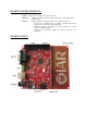
INPUT/OUTPUT: User button with name BUT – connected to STM32F103RBT6 pin.14 PA0.WKUP; Status green LED with name STAT connected to STM32F103RBT6 pin.53 PC12, note that LED-E SMT jumper should be shorted to may LED work properly (it’s shorted by default), if you decide to use PC12 port for other purpose you have to remove the solder short on this jumper which will disconnect the LED from PC12 port; Power supply red LED with name PWR – indicates that 3.
management of the CTS and RTS signals, IrDA SIR ENDEC support, are ISO 7816 compliant and have LIN Master/Slave capability. All USART interfaces can be served by the DMA controller. USART1.Tx – pin.42 PA9 EXT1-4 USART1.Rx – pin.43 PA10 EXT1-7 USART2.Tx – pin.16 PA2 EXT2-7 USART2.Rx – pin.17 PA3 EXT2-10 USART3.Tx – pin.29 PB10 EXT2-14 USART3.Rx – pin.
I2C: STM32F103RBT6 have two I²C bus interfaces which can operate in multi-master and slave modes. They can support standard and fast modes. They support dual slave addressing (7-bit only) and both 7/10-bit addressing in master mode. A hardware CRC generation/verification is embedded. They can be served by DMA and they support SM Bus 2.0/PM Bus. I2C1.SDA – pin.59 PB7 EXT1-15 I2C1.SCL – pin.58 PB6 EXT1-13 I2C1.SMBA – pin.57 PB5 EXT1-12 I2C2.SDA – pin.30 PB11 EXT2-15 I2C2.SCL – pin. 29 PB10 EXT2-14 I2C2.
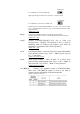
Pin # Signal Name 1 +5V 2 USBDM 3 USBDP 4 GND ADC: STM32F103RBT6 have two 12-bit Analog to Digital Converters which share up to 16 external channels, performing conversions in singleshot or scan modes. In scan mode, automatic conversion is performed on a selected group of analog inputs. Additional logic functions embedded in the ADC interface allow: - Simultaneous sample and hold - Interleaved sample and hold - Single shunt The ADC can be served by the DMA controller.
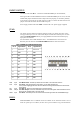
MECHANICAL DIMENSIONS: AVAILABLE DEMO SOFTWARE: DEMO1. Blinking LED for EW-ARM 5.11 Blinks the on-board LED. DEMO2. USB mouse for EW-ARM 5.11 Creates USB mouse and when board is connected to PC it starts moving the mouse cursor in circle. DEMO3. Blinking LED for GCC+OpenOCD+Eclipse Blinks the on-board LED.
ORDER CODE: STM32-P103 – assembled and tested (no kit, no soldering required) How to order? You can order to us directly or by any of our distributors. Check our web www.olimex.com for more info. All boards produced by Olimex are ROHS compliant Revision history: Rev. A - create April 2008 Rev.
Disclaimer: © 2013 Olimex Ltd. All rights reserved. Olimex®, logo and combinations thereof, are registered trademarks of Olimex Ltd. Other terms and product names may be trademarks of others. The information in this document is provided in connection with Olimex products. No license, express or implied or otherwise, to any intellectual property right is granted by this document or in connection with the sale of Olimex products.