User’s Guide Shop online at www.omega.com e-mail: info@omega.
OMEGAnet ® Online Service www.omega.com Internet e-mail info@omega.com Servicing North America: USA: ISO 9001 Certified Canada: One Omega Drive, P.O. Box 4047 Stamford CT 06907-0047 TEL: (203) 359-1660 e-mail: info@omega.com 976 Bergar Laval (Quebec) H7L 5A1, Canada TEL: (514) 856-6928 e-mail: info@omega.
OME-A-8111 Hardware User’s Manual OME-A-8111 Hardware Manual (ver.1.
Table of Contents 1. Introduction_________________________________________________________ 4 1.1 General Description ___________________________________________________ 4 1.2 Features _____________________________________________________________ 4 1.3 Specifications _________________________________________________________ 5 1.3.1 Power Consumption _________________________________________________________ 5 1.3.2 Analog Inputs ______________________________________________________________ 5 1.3.
3. 2.7.2 A/D Conversion Trigger Modes _______________________________________________ 22 2.7.3 A/D Transfer Modes ________________________________________________________ 23 2.7.4 Using software trigger and polling transfer ______________________________________ 23 2.8 D/A Conversion ______________________________________________________ 24 2.9 Analog Input Signal Connection ________________________________________ 25 2.
1. Introduction 1.1 General Description The OME-A-8111 is a high performance, multifunction (analog and digital I/O) board for the PC AT compatible computer with the ISA bus. The OME-A-8111 provides programmable gain (1, 2, 4, 8 and 16). The OME-A-8111 contains a 12-bit ADC with up to 8 single-ended analog inputs. The maximum sample rate of the A/D converter is about 30K sample/sec.
1.3 Specifications 1.3.1 Power Consumption z z z +5V @ 300 mA maximum +12V @ 60 mA maximum -12V @ 30 mA maximum z Operating temperature: 0°C ~ 50°C 1.3.2 z z z z z Channels: 8 single-ended Input range: (software programmable) Bipolar: ±5 V, ±2.5 V, ±1.25 V, ±0.625 V, ±0.3125 V Input current: 250 nA max (125 nA typical) at 25°C On-chip sample and hold Over voltage: continuous single channel to 70Vp-p 1.3.
1.3.4 z z z z z z DA Converter Channels : 1 independent Type : 12-bit multiplying , Analog device AD-7948 Linearity : ± 1/2 bit Output Range : 0~5 V or 0~10 V jumper selected , may be used with other AC or DC reference input. Maximum output limit ± 10V Output Drive : ± 5 mA Settling Time : 0.6 microseconds to 0.01% for full scale step 1.3.5 Digital I/O z z Output port Input port 1.3.
1.3.7 z z z z z Type : 82C54 -8 programmable timer/counter Counters: The counter1 and counter2 are cascaded as a 32-bit pacer timer. Pacer output : 0.00047 Hz to 0.5 MHz Input Gate : TTL compatible Internal Clock : 2 MHz 1.3.8 z z z z z z z z Programmable Timer/Counter Applications Signal analysis FFT & frequency analysis Transient analysis Production test Process control Vibration analysis Energy management Industrial and laboratory measurement and control 1.
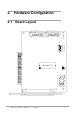
2. Hardware Configuration 2.1 Board Layout 8111 2 20 C N3 D/C O UT 1 19 2 20 1 19 C N2 D/C IN BASS ADDRESS ON 1 2 3 4 5 6 A ( 9 8 7 6 5 4) SW1 A31 BB A D S-774 P1 JP1 JP2 VR1 VR2 VR3 VR4 VR5 A1 CN1 ANA I/0 OME-A-8111 Hardware Manual (ver.1.
2.2 I/O Base Address Setting The OME-A-8111 occupies 16 consecutive locations in I/O address space. The base address is set by DIP switch SW1.
The PC I/O port mapping is given below. ADDRESS DEVICE ADDRESS DEVICE 000-1FF PC reserved 320-32F XT Hard Disk 200-20F Game/control 378-37F Parallel Printer 210-21F XT Expansion Unit 380-38F SDLC 238-23F Bus Mouse/Alt.
2.4 I/O Register Address The OME-A-8111 occupies 16 consecutive PC I/O addresses. The following table lists the registers and their locations.
2.4.1 The 8254 Counter The 8254 Programmable timer/counter has 4 registers from Base+0 through Base+3. For detailed programming information about the 8254, please refer to Intel‘s “Microsystem Components Handbook”. Address Read Write Base+0 8254 Counter 0 8254 Counter 0 Base+1 8254 Counter 1 8254 Counter 1 Base+2 8254 Counter 2 8254 Counter 2 Base+3 Reserved 8254 Counter Control 2.4.
2.4.3 D/A Output Latch Register (WRITE) Base+4: Channel 1 D/A Low Byte Data Format Bit 7 Bit 6 Bit 5 Bit 4 Bit 3 Bit 2 Bit 1 Bit 0 D7 D6 D5 D4 D3 D2 D1 D0 (WRITE) Base+5: Channel 1 D/A High Byte Data Format Bit 7 Bit 6 Bit 5 Bit 4 Bit 3 Bit 2 Bit 1 Bit 0 X X X X D11 D10 D9 D8 D/A 12 bit output data: D11…D0, D11 = MSB, D0 = LSB, X = don‘t care The D/A converter will convert the 12 bits of digital data to analog output.
2.4.5 Clear Interrupt Request (WRITE) Base+8: Clear Interrupt Request Format Bit 7 Bit 6 Bit 5 Bit 4 Bit 3 Bit 2 Bit 1 Bit 0 X X X X X X X X X = don‘t care, XXXXXXXX = any 8 bit data is valid If OME-A-8111 is working in the interrupt transfer mode, an on-board hardware status bit will be set after each A/D conversion. This bit must be cleared by the software before next hardware interrupt.
2.4.7 A/D Multiplex Control Register (WRITE) Base+A : A/D Multiplexer Control Register Format Bit 7 Bit 6 Bit 5 Bit 4 Bit 3 Bit 2 Bit 1 Bit 0 X X X X X D2 D1 D0 A/D input channel selection data =3 bits: D2...D0, D2=MSB, D0=LSB, X=don‘t care Channel Bit_2 Bit_1 Bit_0 0 0 0 0 1 0 0 1 2 0 1 0 3 0 1 1 4 1 0 0 5 1 0 1 6 1 1 0 7 1 1 1 NOTE: The settling time of the multiplexer depends on the source resistance of input sources. Approx. Source resistance = 0.
2.4.
The pacer trigger can control the sampling rate very precisely. So the converted data can be used to reconstruct the waveform of the analog input signal. In pacer trigger mode, the pacer timer will periodically generate trigger signals to the A/D converter. This converted data can be transfer to the CPU by polling or interrupt or DMA transfer method. The software driver provides three polling or interrupt-transfer methods.
2.4.10 D/O Output Latch Register (WRITE) Base+D: D/O Output Latch Low Byte Data Format Bit 7 Bit 6 Bit 5 Bit 4 Bit 3 Bit 2 Bit 1 Bit 0 D7 D6 D5 D4 D3 D2 D1 D0 (WRITE) Base+E: D/O Output Latch High Byte Data Format Bit 7 Bit 6 Bit 5 Bit 4 Bit 3 Bit 2 Bit 1 Bit 0 D15 D14 D13 D12 D11 D10 D9 D8 D/O 16 bits output data: D15...D0, D15=MSB, D0=LSB The OME-A-8111 provides 16 TTL compatible digital outputs. The low 8 bits are stored in address BASE+D.
2.5 Digital I/O The OME-A-8111 provides 16 digital input channels and 16 digital output channels. All levels are TTL compatible. The connections diagram and block diagram are given below: Output Latch Register Base+D Read CN3 D0...D7 1...8 D0...D7 TTL DGND 17...18 DGND D8...D15 DO 9...16 OME-DB-16R Base+E Read 16-Channel Isolated Input Board (Option) Output Latch Register OME-A-8111 Input Buffer Register OME-A-8111 Base+6 Read D0...D7 D0...D7 D8...D15 Base+7 CN2 1...8 TTL 17...
2.6 8254 Timer/Counter The 8254 Programmable timer/counter has 4 registers from Base+0 through Base+3. For detailed programming information about 8254, please refer to Intel‘s “Microsystem Components Handbook”. The block diagram is as below. Gate Cin Cout Counter 0 PACER CLK Cin: clock input Cout: clock output INTCLK: internal clock VCC Counter 1 Cin Gate Cout 10K Counter 2 2M INTCLK Cin Gate Cout Counter0, counter1 and counter2 are all 16 bit counters.
2.7 A/D Conversion This section explains how to perform A/D conversions. The A/D conversion can be performed by software trigger by pacer trigger. At the end of the A/D conversion, it is possible to transfer data by polling and interrupt before using the A/D conversion function; users should notice the following issues: z z z z A/D data register, BASE+4/BASE+5, stores the A/D conversion data (sec. 2.4.2) A/D gain control register, BASE+9, select gain (sec. 2.4.6) (sec. 2.4.
2.7.1 A/D conversion flow Then the user must decide which A/D conversion mode will be used. The software driver supports three different modes. The user can control the A/D conversion by polling mode very easily (sec. 2.4.9). It is recommended to use the software driver if using interrupt or DMA mode. The analog input signals come from CN1. The multiplexer can accept 8 single-ended lines into the gain control module. The gain control module also needs settling time if the gain control code changed.
2.7.3 A/D Transfer Modes OME-A-8111 supports two transfer modes. 1 : polling transfer : This mode can be used with all trigger modes. Detailed information is given in section 2.4.8.The software scans A/D high byte data register, BASE+5, until READY_BIT=0.The low byte data is also ready in BASE+4. 2 : interrupt transfer : This mode can be used with pacer trigger or external trigger. Detailed information is given in section 2.4.8.The user can set the IRQ level by register mode.
2.8 D/A Conversion The OME-A-8111 provides two 12-bit D/A converters. Before using the D/A conversion function, user should notice the following issues: z z D/A output register, BASE+4/BASE+5/BASE+6/BASE+7 (sec. 2.4.3). JP1/JP2 selects internal/external reference voltage (sec. 2.4.1). NOTE: The DA output latch registers are designed as a “double buffered” structure. The user must send the low byte data first, then send the high byte data to store the DA 12-bit digital data.
2.9 Analog Input Signal Connection FIG 1: Connecting analog input configuration OME-A-8111 A/D CH0 A/D CHn Es AGND Signal Shielding z z Signal shielding connections are shown in Fig1. Use single-point connection to frame ground (not AGND or DGND) OME-A-8111 AGND DGND Vin Frame Ground OME-A-8111 Hardware Manual (ver.1.
2.10 Pin Assignment The OME-A-8111 provides three connectors. Connect 1, CN1 functions for analog input & analog output input. Connector 2, CN2, functions as 16 digital outputs. Connector 3, CN3, function as a digital output. CN1/CN2/CN3 Pin Assignment CN1: Analog input/Analog output/Connect Pin Assignment.
CN2: Analog input/Analog output/Connect Pin Assignment.
2.11 Daughter Board The OME-A-8111 can be connected with many different daughter boards. The function of these daughter boards is described as follows. 2.11.1 OME-CA-4002 The OME-CA-4002 is a 37-pin D-Sub male connector. It can directly connect to a 37-pin D-sub connector. 2.11.2 OME-DB-16P The OME-DB-16P is a 16-channel isolated digital input board. The OME-A-8111 provides a 16 channel, non-isolated, TTL-compatible digital inputs from CN2.
3. Calibration The OME-A-8111 is calibrated to its best state of operation. For environments with large vibration, recalibration is recommended. Before calibrating the OME-A-8111, users should have the following items: z z z One 6-digit multi-meter. One stable voltage source (4.9988V) Diagnostic program: this program is included in the delivered package and will guide the user to in proceeding with the calibration. 3.1 Calibration VR Description There are seven VRs on the OME-A-8111.
3.2 D/A Calibration Steps 1. 2. 3. 4. 5. Run A8111CAL.EXE Connect D/A channel0,, pin 30 of CN1 to DVM Adjust VR1 until DVM=5.0000V Press “Enter" key Adjust VR2 until DVM=0.0000V 3.3 A/D Calibration Steps 1. Press “Enter" key 2. Connot A/D Channel 0 to analog ground, CN1-Pin1 to CN1-Pin20. 3. Input stable DC 4.9988V to A/d channel 1, pin2 of CN1. 4. Connect DVM to TP1(-) & (+). 5. Adjust VR5 until DVM=0.0000V. 6. Press Key. 7. Adjust VR4 until A/D data shows 4094 or 4095. 8. Press Key 9.
WARRANTY/DISCLAIMER OMEGA ENGINEERING, INC. warrants this unit to be free of defects in materials and workmanship for a period of 13 months from date of purchase. OMEGA’s WARRANTY adds an additional one (1) month grace period to the normal one (1) year product warranty to cover handling and shipping time. This ensures that OMEGA’s customers receive maximum coverage on each product. If the unit malfunctions, it must be returned to the factory for evaluation.
Where Do I Find Everything I Need for Process Measurement and Control? OMEGA…Of Course! Shop online at www.omega.