PCI-DIO96 DIGITAL INPUT/OUTPUT User’s Manual Revision 2 November, 2000
TABLE OF CONTENTS 1 INTRODUCTION . . . . . . . . . . . . . . . . . . . . . . . . . . . . . . . . . . . . . . . . . . . . . . 1 2 INSTALLATION . . . . . . . . . . . . . . . . . . . . . . . . . . . . . . . . . . . . . . . . . . . . . . . 2 3 I/O CONNECTIONS . . . . . . . . . . . . . . . . . . . . . . . . . . . . . . . . . . . . . . . . . . . 2 3.1 CABLES AND SCREW TERMINAL BOARDS . . . . . . . . . . . . . 2 3.2 CONNECTOR DIAGRAM . . . . . . . . . . . . . . . . . . . . . . . . . . . . . . . . . . 3 3.
This page is blank.
1 INTRODUCTION The PCI-DIO96 is a 96-bit line digital I/O board. The board provides the 96 bits in four 24-bit groups. Each group provides an 8-bit port A and port B, as well as an 8-bit port C that can be split into independent 4-bit port C-HI and a 4-bit port C-LO. See Figure 1-1 below. On power up and reset, all I/O bits are set to input mode. If you are using the board to control items that must be OFF on reset, you will need to install pull-down resistors.
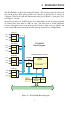
2 INSTALLATION The PCI-DIO96 boards are completely plug-and-play. There are no switches or jumpers on the board. All board addresses are set by your computer’s plug-and-play software. InstaCal is the installation, calibration and test software supplied with your data acquisition / IO hardware. Refer to the Extended Software Installation Manual to install InstaCal. If you need it, there is some on-line help in the InstaCal program.
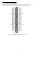
3.2 CONNECTOR DIAGRAM The PCI-DIO96 I/O connector is a 100-pin type connector accessible from the rear of the PC at the expansion backplate See Figure 3-1 below for the board pin out.
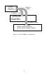
BOARD’S 100-PIN I/O CONNECTOR C100FF-xx CABLE I/O PINS 1 TO 50 SIGNAL CONDITIONING or 50-PIN SCREW TERMINAL BOARD. I/O PINS 51 TO 100 SIGNAL CONDITIONING OR 50-PIN SCREW TERMINAL BOARD Figure 3-2.
DIO Group 3 DIO Group 2 Port A6 D Port A4 D Port A2 D Port A0 D Port B6 D Port B4 D Port B2 D Port B0 D Port C6 D Port C4 D Port C2 D Port C0 D Port A6 C Port A4 C Port A2 C Port A0 C Port B6 C Port B4 C Port B2 C Port B0 C Port C6 C Port C4 C Port C2 C Port C0 C Ground 2 4 6 8 10 12 14 16 18 20 22 24 26 28 30 32 34 36 38 40 42 44 46 48 50 1 3 5 7 9 11 13 15 17 19 21 23 25 27 29 31 33 35 37 39 41 43 45 47 49 Port A7 D Port A5 D Port A3 D Port A1 D Port B7 D Port B5 D Port B3 D Port B1 D Port C7 D Port
3.3 SIGNAL CONNECTION CONSIDERATIONS All the digital inputs on the PCI-DIO96 are 8255 CMOS TTL. The PCI-DIO96 output signals are 8255 CMOS. OMEGA Engineering Inc. offers a wide variety of digital signal conditioning products that provide an ideal interface between high voltage and/or high current signals and the PCI-DIO96.
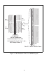
3.4 CIO-ERB24 & SSR-RACK24 CONNECTIONS PCI-DIO96 PCI-DIO96 boards provide digital I/O in two major groups of 48 bits each (96 total, but each side of the C100FF-xx cable provides 48 bits). However, many popular relay and SSR boards provide only 24-bits of I/O. The CIO-ERB24 and SSR-RACK24 each implements a connector scheme where all 96 bits of the PCI-DIO96 board may be used to control relays and/or SSRs. This configuration is shown in Figure 3-4 below.
4 SOFTWARE We highly recommend that users take advantage of our Universal Library package's easy-to-use programming interfaces. However, if you are an experienced programmer, and wish to read and write directly to the board, we have provided a detailed register map in the next chapter. 4.1 UNIVERSAL LIBRARY The Universal Library provides complete access to the PCI-DIO96 functions from a range of programming languages.
5 REGISTER MAPS The PCI Controller, a PLX-9052, has four configuration, control, and status registers (Table 5-1). They are described in the following section. I/O Region BADR0 BADR1 BADR2 BADR3 Table 5-1. I/O Region Register Operations Function Operations PCI memory-mapped configuration 32-bit double word registers PCI I/O-mapped config. registers 32-bit double word N/A N/A Digital I/O registers 8-bit byte 5.1 BADR0 BADR0 is reserved for the PLX-9052 configuration registers.
INTE Interrupt enable (local): 0 = disabled, 1 = enabled (default) INTPOL Interrupt polarity: 0 = active low (default), 1 = active high INT Interrupt status: 0 = interrupt not active, 1 = interrupt active PCINT PCI interrupt enable: 0 = disabled (default), 1 = enabled LEVEL/EDGE Interrupt trigger control: 0 = level triggered mode (default), 1 = edge triggered mode INTCLR Interrupt clear (edge triggered mode only): 0 = N/A, 1 = clear interrupt ISAMD ISA mode enable control (must be set to 1) 0 =
5.4 BADR3 BADR3 is an 8-bit data bus for reading, writing and control of the individual 82C55 chips and the 82C54. Refer to Table 5-2 for register offsets. REGISTER BADR3 + 0 BADR3 + 1 BADR3 + 2 BADR3 + 3 BADR3 + 4 BADR3 + 5 BADR3 + 6 BADR3 + 7 BADR3 + 8 BADR3 + 9 BADR3 + A BADR3 + B BADR3 + C BADR3 + D BADR3 + E BADR3 + F BADR3 + 10h BADR3 + 11h BADR3 + 12h BADR3 + 13h BADR3 + 14h BADR3 + 15h Table 5-2.
GROUP 0, PORT B DATA BADR3 + 1 READ/WRITE 7 6 5 D7 D6 D5 GROUP 0, PORT C DATA BADR3 + 2 READ/WRITE 7 6 5 4 3 2 1 0 D4 D3 D2 D1 D0 4 3 2 1 0 C8 C7 C6 C5 C4 C3 C2 C1 CH4 CH3 CH2 CH1 CL4 CL3 CL2 CL1 4 3 2 1 0 A CH M1 B CL GROUP 0 CONFIGURE BADR3 + 3 READ/WRITE 7 6 5 MS M3 M2 This register is used to configure the Group 0 ports as either input or output, and configures the operating mode to mode 0, 1 or 2. The following describes configuration for mode 0.
D4 0 0 0 0 0 0 0 0 1 1 1 1 1 1 1 1 Table 5-3.
GROUP 1 CONFIGURE BADR3 + 7 READ/WRITE 7 6 5 MS M3 M2 4 3 2 1 0 A CH M1 B CL 5.4.
GROUP 3, PORT B DATA BADR3 + D hex READ/WRITE 7 6 5 D7 D6 D5 GROUP 3, PORT C DATA BADR3 + E hex READ/WRITE 7 6 5 4 3 2 1 0 D4 D3 D2 D1 D0 4 3 2 1 0 C8 C7 C6 C5 C4 C3 C2 C1 CH4 CH3 CH2 CH1 CL4 CL3 CL2 CL1 4 3 2 1 0 A CH M1 B CL GROUP 3 CONFIGURE BADR3 + F hex READ/WRITE 7 6 5 MS M3 M2 5.4.
COUNTER CONFIGURATION BADR3 + 13 hex READ/WRITE 7 6 5 D7 D6 D5 4 3 2 1 0 D4 D3 D2 D1 D0 This register is used to set the operating modes of each of the 82C54’s counters. Configure the counters by writing mode information to the Configure register, followed by the count information written to the specific counter (data) registers. Refer to the Celeritous 82C54 data sheets for more detailed information. 5.4.
5.4.7 Counter Interrupt Source Configure BADR3 + 15 hex READ/WRITE 7 6 X X 5 4 3 2 1 0 X X X INTEN CTRIR CTR1 INTEN Enables or disabled interrupts. 1 = enabled, 0 = disabled CTRIR Enables or disables the counters as an interrupt source. 1 = counters may generate interrupts. 0 = counters cannot generate interrupts. CTR1 Controls whether counter 2 is the interrupt source, or counter 1 is the interrupt source.
6 SPECIFICATIONS Power Consumption +5V 150 mA max Digital Input / Output Digital Type Number of I/O Configuration per 82C55 Output High Output Low Input High Input Low Power-up / reset state Pull-Up/Pull-Down Resistors Four 82C55 96 • 2 banks of 8 and 2 banks of 4, or • 3 banks of 8, or 2 banks of 8 with handshake 3.0 volts min @ −2.5mA 0.4 volts max @ 2.5mA 2.0 volts min, 5.5 volts absolute max 0.8 volts max, −0.5 volts absolute min Input mode (high impedance) User installed.
Interrupts The interrupt control registers function with the four 82C55 devices and the 82C54 counter timer to provide interrupt sources. Interrupt PCI Interrupt enable Interrupt polarity INTA# - mapped to IRQn via PCI BIOS at boot-time Programmable through PLX9052 INTCSR High or low level. Programmable through PLX9052 Rising / falling edge. Programmable through PLX-9052 1.
7 ELECTRONICS AND INTERFACING This brief introduction to the electronics most often needed by digital I/O board users covers a few key concepts. IMPORTANT NOTE WHENEVER AN 82C55 IS POWERED-ON OR RESET, ALL PINS ARE SET TO HIGH-IMPEDANCE INPUT. FOLLOWING STANDARD TTL FUNCTIONALITY, THESE INPUTS WILL TYPICALLY FLOAT HIGH, AND MAY HAVE ENOUGH DRIVE CURRENT TO TURN ON EXTERNAL DEVICES.
If the board is in output mode, the board has enough power to override the pull-up/down resistor's high signal and drive the line to 0 volts. If the output circuit asserts a high signal, the pull-up resistor guaranties that the line goes to +5 V. Of course, a pull-down resistor accomplishes the same task except that the line is pulled low when the board is reset. The board has enough power to drive the line high.
The most convenient way to use solid state relays and a PCI-DIO96 board is to use a Solid State Relay Rack. An SSR Rack is a circuit board with input buffer amplifiers that are powerful enough to switch the SSRs. The buffer amplifiers and SSRs are socketed. The standard buffer amplifiers are inverting types, meaning that a low input from a DIO 82C55 outputs a high to the SSR which turns it on (“closes” the SSR output). If desired, non-inverting amplifiers can be specified. 7.
with a full scale range of 0 to 5 volts, the Attenuation is 2:1, or just 2. R1=(A-1)*R2 For a given attenuation, pick a handy resistor and call it R2, then use this formula to calculate R1. Digital inputs can readily use voltage dividers. For example, if you wish to measure a digital signal that is at 0 volts when off and 24 volts when on, you cannot connect that directly to the PCI-DIO96 digital inputs. The voltage must be dropped to 5 volts max when on. The Attenuation is 24:5 or 4.8.
For Your Notes 24
For Your Notes 25
For Your Notes 26
EC Declaration of Conformity PCI-DIO96 Part Number Digital I/O board Description to which this declaration relates, meets the essential requirements, is in conformity with, and CE marking has been applied according to the relevant EC Directives listed below using the relevant section of the following EC standards and other normative documents: EU EMC Directive 89/336/EEC: Essential requirements relating to electromagnetic compatibility.
OMEGA Engineering Inc. One OMEGA Drive Stamford, CT 06801 (800) 872-9436 Fax: (203) 359-7700 E-mail: info@omega.com www. omega.