User’s Guide Shop online at www.omega.com e-mail: info@omega.
OMEGAnet ® Online Service www.omega.com Internet e-mail info@omega.com Servicing North America: USA: ISO 9001 Certified Canada: One Omega Drive, P.O. Box 4047 Stamford CT 06907-0047 TEL: (203) 359-1660 e-mail: info@omega.com 976 Bergar Laval (Quebec) H7L 5A1, Canada TEL: (514) 856-6928 e-mail: info@omega.
Table of Contents 1. 2. 3. 4. INTRODUCTION................................................................................................................................. 5 1.1 GENERAL DESCRIPTION ............................................................................................................ 5 1.2 THE BLOCK DIAGRAMS................................................................................................................. 6 1.3 FEATURES ...........................................
.2 THE 8254 TIMER ........................................................................................................................ 36 4.3 THE A/D TRIGGER ..................................................................................................................... 36 4.4 A/D CONVERSION ....................................................................................................................... 38 4.4.1 A/D Conversion Trigger Modes.............................................
1. Introduction The OME-PCI-1002H/L card provides 12-bit ADC and two 16-bit digital I/O ports. 1.1 General Description The OME-PCI-1002L and OME-PCI-1002H are high performance multifunction cards, with A/D and digital I/O for PC and compatible computers in a 5V PCI slot. This family has the following features: one 12-bit 110K A/D converter, 16 channels D/I, 16 channels D/O, programmable interrupt source and true “Plug and Play” support.
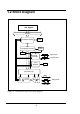
1.2 Block Diagram X86 System PCI BUS EPROM PCI Interface System Status Control Local System Controller Interrupt Digital Inputs 16 bits DI 16 bits DO Pacer Generator Digital Outputs 4MHz A/D control logic A/D Data Buffer 12-bit A/D Converter Gain Mux Figure 1-1. The OME-PCI-1002 series block diagram.
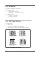
1.3 Features • Bus: 5V PCI (Peripherals Component Interface) bus. 1. • • • • • A/D: One A/D converter with maximum 110K samples/second. 32 single-ended / 16 differential programmable inputs for OME-PCI-1002L/H. Three different A/D trigger methods. Three different external trigger methods. Programmable gain control, programmable offset control. 2. DIO: • 16 digital inputs and 16 digital outputs (TTL compatible). • High-speed data transfer rate: 2.7M word/sec (non-burst mode). 3.
1.4 Specifications 1.4.1 Power Consumption • • +5V @ 960mA maximum, OME-PCI-1002L/H Operating temperature : 0°C to +70°C 1.4.2 Analog Inputs • • • • • • • Channels: ( software programmable ) 32 single-ended inputs/16 differential inputs, jumper selectable. Gain control : ( software programmable ) OME-PCI-1002H, Gains - 1, 10, 100, 1000. OME-PCI-1002L, Gains - 1, 2, 4, 8. Input signal range : OME-PCI-1002L: Bipolar Range: ±10, ±5V, ±2.5V, ±1.25V OME-PCI-1002H: Bipolar Range: ±10, ±1V, ±0.1V, ±0.
1.4.3 D/I and D/O • • Channels: 16 channels DI, 16 channels DO DO: Digital output port Output level: TTL compatible Output current: • Ioh = 0.5mA, Iol = 8mA DI: Digital input port Input level: TTL compatible Input current: 50uA (max) 1.4.4 A/D Trigger Methods • Trigger-methods : 1. Software trigger 2. Pacer trigger: 16-bit programmable timer/counter 3.
1.4.5 Interrupt Channel • • • Interrupt: INTA (Automatically assigned by PCI-controller). Enable/Disable: Via PCI control register and add-on control register. Interrupt source: (Selected by on-board control register) 1. A/D conversion interrupt 2. Pacer 0 interrupt (Timer 0) 3. Pacer 1 interrupt (Timer 1) 4. External interrupt 1. End of Conversion 2. Pacer 0 A/D busy IRQ IRQ 3. Falling edge of Pacer 0 Falling edge of External trigger 4.
1.5 Applications z z z z z z z z Signal analysis. FFT & frequency analysis. Transient analysis. Speech analysis. Temperature monitor. Vibration analysis. Energy management. Industrial and laboratory measurement and control. Signal Analysis Multi-I/O signals Transition Temperature Frequency Other Laboratory use Process Control OME-PCI-1002 series Speech Analysis Vibration PCI interface Single-task or multitask Figure 1-4. OME-PCI-1002 series multifunction cards.
1.6 Product Check List In addition to this manual, the package includes the following items: • One OME-PCI-1002 card • One CD-ROM Release Notes The release notes contain the latest information updates. We strongly suggest that you read them first.
2. Hardware Configuration 2.1 Board Layout CON3 CON2 Figure 2-1. OME-PCI-1002 board layout.
2.2 Jumper Setting There is only one jumper on the OME-PCI-1002. JP1 is used to select the analog input type. For single-ended inputs, users should connected pin 1, 3 and pin 2, 4. For differential inputs, Pin 3, 5 and Pin 4, 6 should be connected. JP1 JP1 1 2 5 6 Single-ended Inputs (Default) 1 2 5 6 Differential Inputs 2.3 A/D Calibration • A/D Calibration for OME-PCI-1002 card Step 1: Apply +10V to channel 0. Step 2: Apply +0V to channel 1. Step 3: Apply -10V to channel 2. Step 4: Run DEMO6.
2.4 System Block Diagram D/I D/O 8254 Timer A/D Buffer Data PCI Interface Controller Adr Interrupt controller A/D Trigger Logic Dispatch controller NVRA External Trigger PCI BUS Figure 2-2. OME-PCI-1002 System Function Block. 15 A/D Converter Multiplexers, Gain Amp. Scale Adj.
2.5 Daughter Boards 2.5.1 OME-DB-1825 The OME-DB-1825 is a daughter board designed for 32-channel AD cards such as the OME-PCI-1002. Refer to the OME-DB-1825 user manual for details. 37pin cable 2.5.2 OME-DB-8225 The OME-DB-8225 provides a on-board CJC (Cold Junction Compensation) circuit for thermocouple measurement and a terminal block for easy signal connection. The CJC is connected to A/D channel_0. The OME-PCI-1002 can connect CON3 direct to the OME-DB-8225 through a 37-pin D-sub connector.
2.5.5 OME-DB-16P Isolated Input Board The OME-DB-16P is a 16-channel isolated digital input daughter board. The optically isolated inputs of the OME-DB-16P consist of a bi-directional optocoupler with a resistor for current sensing. You can use the OME-DB-16P to sense DC signal from TTL levels up to 24V or use the OME-DB-16P to sense a wide range of AC signals.
2.5.6 OME-DB-16R Relay Board The OME-DB-16R, 16-channel relay output board consists of 16 form C relays that can be switched under program control. Applying 5 volts to the appropriate relay channel through the 20-pin flat connector can energize the relays. Each relay has its own LED that will light when the relay is energized. To avoid overloading your PC’s power supply, the board provides screw terminals for external power. Note: Channel: 16 Form C Relay Relay: Switching up to 0.
2.6 Analog Input Signal Connection The OME-PCI-1002 can measure signals in the single-ended or differential mode. In the differential mode each channel has a unique signal HIGH and signal LOW connection. In the single-ended mode all channels have a unique signal HIGH connection but share a common LOW or ground connection. Differential connections are very useful for low level signals (millivolt), since they better reject electrical noise that can affect the quality of the measurement.
Figure 2-3A If the source is grounded, a second ground connection on the card could result in a ground loop.
Figure 2-4 Figure 2-5 21
Figure 2-6 R is a shunt resistor. A 250Ω shunt resistor converts 4-20mA to 1-5Vdc. Signal Shielding z z The signal shielding connections in Figure 2-3 to Figure 2-6 are all the same Use a single connection to frame ground (not A.GND or D.GND) OME-PCI-1002 A.GND D.
2.7 Jumper Settings There is only one jumper on the OME-PCI-1002. JP1 is used to select the analog input type. For single-ended inputs, users should connect Pin-1, 3 and Pin-2, 4. For differential inputs, Pin-3, 5 and Pin-4, 6 should be connected.
2.8 The Connectors CON1: Digital output connector pin assignment.
CON3: Analog input/output connector pin assignment.
3. I/O Registers 3.1 How to Find the I/O Address The Plug & Play BIOS will assign a valid I/O address to all OME-PCI-1002 cards in the system during the computer’s power-on stage. The ID numbers of OME-PCI-1002 are shown below: • Vendor ID • Device ID = 1234 = 1002 Associated Driver Functions: 1. P1002_DriverInit(&wBoard) This function detects the number of OME-PCI-1002 cards in the system. • wBoard=1 Æ only one OME-PCI-1002 in this PC system. • wBoard=2 Æ there are two OME-PCI-1002 in this PC system. 2.
The sample program code is shown below: /* Step1: Detect all OME-PCI-1002 card first */ wRetVal=P1002_DriverInit(&wBoards); printf("There are %d OME-PCI-1002 Cards in this PC\n",wBoards); /* Step2: save resource of all OME-PCI-1002 cards installed in this PC */ for (i=0; i
3.2 The I/O Address Map The OME-PCI-1002 registers are given below. The address of each register is determined by adding the offset to the base address of the corresponding section.
3.2.1 Section 1 Although there are 128 I/O ports used by the on-board PCI interface controller, only one register is used for most applications. The user should not modify the other registers! The PCI interrupt control register (4Ch) controls the interrupts generated by the system.
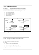
3.2.2 Section 2 This group of registers is used by the add-on control logic. 64 bytes of I/O locations are used. Their detailed descriptions are shown below 3.2.2.1 The 8254 Registers The 8254, programmable timer/counter, is used to generate periodic interrupts, A/D trigger and the machine independent timer. Addresses 00h, 04h, 08h and 0Ch are used to program the 8254. Timer 0 is used as Pacer 0 and timer 1 is used as Pacer 1. Timer 2 is used as the machine independent timer (P1002_Dealy() function).
3.2.2.4 The Status Register Address 10h is used is the status register. Reading from this address will return the data from the status register. The format of status register is: Bit7-6 Bit5 Gain Control 8245 Timer 1 Bit4 Bit3 Bit2 Bit1 Bit0 8245 8245 Analog A/D Busy Reserved Timer 0 Timer 2 input type Bit 7-6: Current A/D gain control. Bit 5 : Output of 8254 timer 1. Bit 4 : Output of 8254 timer 0. Bit 3 : Output of 8254 timer 2. Bit 2 : Reserved. Used for hardware testing.
3.2.2.6 Clear Interrupt Reading from 1Ch will clear the add-on interrupt. 3.2.2.7 The Analog Input Selection Register … Analog inputs The analog input channel selection register uses address 10h and address 14h is used by the analog gain control selection register. Write 0-31 to port 10h to select the channel number (for differential input, write 0-15). Write 0-3 to port 14h to select the gain control. Analog Mux. ADC AMP Select Gain control … Channel select Figure 3-2. Analog input control.
For OME-PCI-1002H: 3. [Bit1,Bit0] [0 0] [0 1] [1 0] [1 1] Gain 1 10 100 1000 These registers are set to 0 after power-on or a hardware reset signal. 3.2.2.8 The General Control Register The general control register (18h) is used to control the add-on interrupt source and the A/D trigger method. The format of this register is: Bit4-2 Bit 1-0 Interrupt source selection register A/D trigger method selection register 3.2.2.8.
3.2.2.8.2 Trigger Method Selection There are several trigger methods that can be selected by the user (see section 1.4.5): [Bit1,Bit0 ] Descriptions [ 0, 0 ] General trigger mode. 8254 timer 0 trigger (internal pacer trigger ) or software trigger. [ 0, 1 ] External clock trigger mode. [ 1, 0 ] Pre-trigger mode. [ 1, 1 ] Post-trigger mode. Note: 1. In the general trigger mode, both the 8254 timer 0 and the software trigger are used as the A/D trigger signals.
4. Function Operation 4.1 Digital I/O The OME-PCI-1002 series provides 16 digital input channels and 16 digital output channels. All signals are TTL compatible. The connector and block diagrams are given below: CN2 BaseAddr+20h read signal. DI port Local Data Bus D0 ... D15 BaseAddr+20h write signal DO port CN1 Figure 4.1. DIO function diagram.
4.2 The 8254 Timer The OME-PCI-1002 series provide 3 independent 16-bit timer/counters. Each timer has a different function. Timer 0 is used as Pacer 0. Timer 1 is used as Pacer 1. Timer 2 is used as the machine independent timer. The block diagram is given as follows: VCC 4 M Hz EN CLK Timer 0 Pacer 0 OUT1 Local Data Bus CLK D0…D7 Timer 1 User EN Pacer 1 OUT2 CLK Status Timer EN 8254 OUT3 Figure 4-2. 8254 Block Diagram. 4.
The A/D trigger logic can initiate an A/D conversion upon an external trigger. Valid external trigger signals must be TTL compatible and meet minimum pulse width requirements. The requirements are shown below: External trigger tdu tre Symbol Name Minimum Maximum Tdu Duration time 40ns ∞ Tre Recover time 100ns ∞ Note: The OME-PCI-1002 is designed only for time sensitive triggers (trigger is dependent only on the time of the falling edge of signal).
4.4 A/D Conversion An A/D conversion can be initiated three different ways: software command, internal programmable interval timer or external trigger. At the end of the A/D conversion, it is possible to transfer the data by polling a status register and reading the data when ready or by generating a hardware interrupt and an interrupt service routine. All modes are selected by a control register on the OME-PCI-1002 and are supported by the utility software.
Before performing A/D conversions, the JP1 jumper should be set for single-ended or differential. The software driver supports both polling and interrupt driven A/D, however, polling is the simplest way to perform an A/D conversion. The settling time of multiplexer depends on the impedance of the signal source. Because the driver does not incorporate the settling time, the user needs to program a delay when switching from one channel to another or when changing gains.
4.4.1 A/D Conversion Trigger Modes The OME-PCI-1002 supports three trigger modes. 1 : Software Trigger : Write any value to A/D software trigger control register, BASE+1Ch, will initiate a A/D conversion cycle. This mode is very simple but very difficult to control sampling rate. 2 : Pacer Trigger Mode : The block diagram of pacer timer is shown in section 3.2. The sample rate of pacer is very precise.
Software Trigger and Polling Techniques The steps below should be followed for software triggering and polling: 1. Send 00h to A/D mode control register (software trigger + polling transfer) 2. Send channel number to multiplexer control register. 3. Send the gain control code value to gain control register. 4. Send any value to software trigger control register to generate a software trigger signal. 5. Scan the READY bit of the A/D high byte data until READY=0 6. Read the 12 bits A/D data. 7.
l=inp(wBaseAddr+2*4); /* delay starting two clks */ h=inp(wBaseAddr+2*4); for (count=32767;count>0;count--){ outp(wBaseAddr+12,0x80); /* latch counter_2 */ l=inp(wBaseAddr+8); h=inp(wBaseAddr+8); if (h>=0x80) return NoError; } return TimeOut; } //-------------------------------------------------------void AdPolling(UCHAR channel, UCHAR gain, WORD delay) { outp(wBaseAddr+0x18,0); // Select Mode 0 outp(wBaseAddr+0x10,channel); outp(wBaseAddr+0x14,gain); P1002_Delay(delay); outp(wBaseAddr+0x1c,01); // A/D
char c; clrscr(); P1002_DriverInit(&wBoards); printf("\n(1) Threr are %d OME-PCI-1002 Cards in this PC",wBoards); if ( wBoards==0 ) { putch(0x07); putch(0x07); putch(0x07); printf("(1) There are no OME-PCI-1002 card in this PC !!!\n"); exit(0); } printf("\n(2) Show the Configuration Space of all OME-PCI-1002:"); for(i=0; i
5. Software and Demo Program 1. Demo programs for DOS • …\1002\BC\LARGE\DEMO> • …\1002\BC\LARGE\LIB> ← demo program ←library and driver • • • • • • DEMO1: Digital output. DEMO2: Digital output and Digital input test by itself. DEMO3: A/D Polling for channel 0. DEMO4: A/D Polling for channel 0,1,2,3 and defferent gain 1,2,4,8. DEMO5: A/D Pacer trigger. DEMO6: A/D Calibration. • DEMO7: Find card number. 2. Demo program for Windows95/98/NT • Refer to CD-ROM.
6. Diagnostic Program 6.
cards. Step 7: If a card’s D/O=D/I Æ this is the physical card number, remember this number. Step 8: Repeat the previous two steps to find the physical card number of all boards. 6.3 D I/O Test Step 1: Power-off the PC. Step 2: Install one OME-PCI-1002 card with a 20-pin flat cable between CON1 & CON2. Step 3: Power-on the PC then run DEMO2.EXE. Step 4: The DO and DI are displayed as TEST OK or TEST ERROR. 6.4 A/D Test • A/D Test for OME-PCI-1002 card Step 1: Power-off the PC.
WARRANTY/DISCLAIMER OMEGA ENGINEERING, INC. warrants this unit to be free of defects in materials and workmanship for a period of 13 months from date of purchase. OMEGA’s WARRANTY adds an additional one (1) month grace period to the normal one (1) year product warranty to cover handling and shipping time. This ensures that OMEGA’s customers receive maximum coverage on each product. If the unit malfunctions, it must be returned to the factory for evaluation.
Where Do I Find Everything I Need for Process Measurement and Control? OMEGA…Of Course! Shop online at www.omega.