User’s Guide Shop online at www.omega.com e-mail: info@omega.
OMEGAnet ® Online Service www.omega.com Internet e-mail info@omega.com Servicing North America: USA: ISO 9001 Certified Canada: One Omega Drive, P.O. Box 4047 Stamford CT 06907-0047 TEL: (203) 359-1660 e-mail: info@omega.com 976 Bergar Laval (Quebec) H7L 5A1, Canada TEL: (514) 856-6928 e-mail: info@omega.
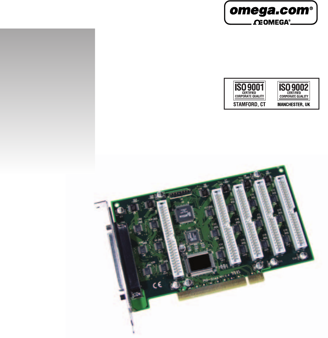
OME-PIO-D144 User’s Manual OME-PIO-D144 User’s Manual (Ver.2.
Table of Contents 1. 2. INTRODUCTION ........................................................................................................................4 1.1 SPECIFICATIONS ..................................................................................................................4 1.2 PRODUCT CHECK LIST ........................................................................................................4 HARDWARE CONFIGURATION ............................................................
4. DEMO PROGRAM....................................................................................................................33 4.1 OME-PIO-D144.H ..............................................................................................................34 4.2 DEMO1: USE D/O OF CN1....................................................................................................35 4.3 DEMO2: USE D/O OF CN1~CN6 ..................................................................................
1. Introduction The OME-PIO-D144 consists of one D-Sub 37 & five 50-pin flat-cable connectors. There are three 8-bit ports - PA, PB & PC - in each connector. Every port consists of 8-bit programmable D/I/O. So the OME-PIO-D144 can provide 144 channels of TTL-compatible D/I/O. 1.
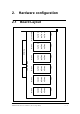
Board Layout 2.1 Hardware configuration 2. CN1_PC CN1_PB CN1_PA CN1 50-PIN CN2_PC CN2_PB CN2_PA CN2 50-PIN CN3_PC CN3_PB CN3_PA CN3 50-PIN CN4_PC CN4_PB CN4_PA CN4 50-PIN CN5_PC CN5_PB CN5_PA CN5 50-PIN CN6_PC CN6_PB CN6_PA CN6 OME-PIO-D144 D-Sub 37 PIN PCI BUS ----- 5 OME-PIO-D144 User’s Manual (Ver.2.
2.2 I/O Port Location There are eighteen 8-bit I/O ports in the OME-PIO-D144. Every I/O port can be programmed as D/I or D/O port. When the PC is first powered up, all eighteen ports are used as D/I ports. The I/O port location is given as following: Connector of OME-PIO-D144 PA0 to PA7 PB0 to PB7 PC0 to PC7 CN1 CN1_PA CN1_PB CN1_PC CN2 CN2_PA CN2_PB CN2_PC CN3 CN3_PA CN3_PB CN3_PC CN4 CN4_PA CN4_PB CN4_PC CN5 CN5_PA CN5_PB CN5_PC CN6 CN6_PA CN6_PB CN6_PC Refer to Sec. 2.
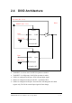
2.4 D/I/O Architecture I/O select (Sec. 3.3.9) D/I/O RESET\ (Sec. 3.3.1) disable\ Data (Sec. 3.3.7) input Latch Clock input D/O latch CKT disable Data (Sec. 3.3.7) Buffer input Clock input D/I buffer CKT • • • • • The RESET\ is in Low-state Æ all D/I/O operation is disable The RESET\ is in High-state Æ all D/I/O operation is enable.
2.5 Interrupt Operation The PC0, PC1, PC2, PC3 of CN1_PC can be used as interrupt signal source. Refer to Sec. 2.1 for PC0/1/2/3 location. The interrupt of OME-PIO-D144 is level-trigger & Active_High. The interrupt signal can be programmed to inverted or noninverted state. The programming procedure is as follows: 1. make sure the initial level is High or Low 2. if the initial state is High Æ select the inverted signal (Section. 3.3.6) 3.
Example 1: assume initial level=Low, PC0 is used as interrupt source: Initial=Low Iniaial_sub() { now_int_state=0 _outpd(wBase+0x2a,0) /*(select the non-inverted signal)*/ ISR_sub() { If (now_int_state==0) /* old state=low Æ change to high now */ { now_int_state=1; /* now int_signal is High */ /*** application codes are given here ***/ _outpd(wBase+0x2a,1); /* select the inverted signal */ } else /* old state=highÆ change to low now */ { now_int_state=0; /* now int_signal is Low */ /*** application code
Example 2: assume initial level=High, PC0 is used as interrupt source: Initial=High Inverted=Low Iniaial_sub() { now_int_state=1 _outpd(wBase+0x2a,1) /*(select the inverted signal)*/ ISR_sub() { If (now_int_state==0) /* old state=low Æ change to high now */ { now_int_state=1; /* now int_signal is High */ /*** application codes are given here ***/ _outpd(wBase+0x2a,1); /* select the inverted signal */ } else /* old state=highÆ change to low now */ { now_int_state=0; /* now int_signal is Low */ /*** app
Example 3: assume CN1_PC0 is initial Low, active High, CN1_PC1 is initial High, active Low CN1_PC2 is initial Low, active High CN1_PC3 is initial High, active Low As follows: CN1_PC0 CN1_PC1 CN1_PC2 CN1_PC3 CN1_PC0 & CN1_PC1 are active at the same time. CN1_PC0 & CN1_PC1 are return to normal at the same time. CN1_PC2 & CN1_PC3 are active at the same time. CN1_PC2 & CN1_PC3 are return to normal at the same time. Refer to DEMO5.C for source program.
void interrupt irq_service() { char cc; int_num++; /* 1. Read interrupt signal status */ new_int_state=inp(wBase+0x07)&0xff; /* 2. Find the active signal */ int_c=new_int_state ^ now_int_state; /* 3. IF PC0 is active */ if ((int_c&0x01) != 0) { cc=new_int_state&0x01; if (cc !=0) CNT_H1++; else CNT_L1++; invert=invert ^ 1; } /* 4. IF PC1 is active */ if ((int_c&0x02) != 0) { cc=new_int_state&0x02; if (cc !=0) CNT_H2++; else CNT_L2++; invert=invert ^ 2; } /* 5.
2.6 Daughter Boards 2.6.1 OME-DB-37 The OME-DB-37 is a general purpose daughter board with D-sub 37 pin connector. It is designed for easy wire connection. 37-PIN cable OME-DB-37 2.6.2 OME-DN-37 & OME-DN-50 The OME-DN-37 is a general purpose daughter board for D-sub 37 pin connector. The OME-DN-50 is designed for 50-pin flat-cable header. They are designed for easy wire connection. Both boards are DIN rail mountable. 37-PIN cable OME-DN-37 2.6.
2.6.4 OME-ADP-37/PCI & OME-ADP-50/PCI The OME-ADP-37/PCI & OME-ADP-50/PCI are extenders for the 50-pin headers. One side of the OME-ADP-37/PCI & OME-ADP-50/PCI can be connected to a 50-pin header. The other side can be mounted on the PC chassis as following: OME-ADP-37/PCI: 50-pin header to D-Sub37 extender. OME-ADP-50/PCI: 50-pin header to 50-pin header extender. OME-PIO-D144 User’s Manual (Ver.2.
2.6.5 OME-DB-24P/24PD Isolated Input Board The OME-DB-24P is a 24 channel isolated digital input daughter board. The optically isolated inputs of the OME-DB-24P consist of a bi-directional opto-coupler with a resistor for current sensing. You can use the OME-DB-24P to sense DC signal from TTL levels up to 24V or use the OME-DB-24P to sense a wide range of AC signals.
2.6.6 OME-DB-24R/24RD Relay Board The OME-DB-24R, 24 channel relay output board, consists of 24 form C relays for efficient switching of load via programmed control. The relay are energized by apply 12V/24V signal to the appropriated relay channel on the 50-pin flat connector. There are 24 enunciator LED’s for each relay and they light when their associated relay is activated.
2.6.7 OME-DB-24PR/24POR/24C OME-DB-24PR 24 × power relay, 5A/250V OME-DB-24POR 24 × Photo MOS relay, 0.1A/350VAC OME-DB-24C 24 × open collector, 100mA per channel, 30V max. The OME-DB-24PR, 24 channel power relay output board, consists of 8 form C and 16 form A electromechanical relays for efficient switching of load via programmed control. The contact of each relay can control a 5A load at 250ACV/30VDCV.
2.6.8 Daughter Board Comparison Table 20-pin flat-cable 50-pin flat-cable D-sub 37-pin OME-DB-37 No No Yes OME-DN-37 No No Yes OME-ADP-37/PCI No Yes Yes OME-ADP-50/PCI No Yes No OME-DB-24P No Yes No OME-DB-24PD No Yes Yes OME-DB-16P8R No Yes Yes OME-DB-24R No Yes No OME-DB-24RD No Yes Yes OME-DB-24C Yes Yes Yes OME-DB-24PRD No Yes Yes OME-DB-24POR Yes Yes Yes OME-DB-24SSR No Yes Yes OME-PIO-D144 User’s Manual (Ver.2.
2.7 Pin Assignment CN1: 37-PIN of D-type female connector. Pin Number Description Pin Number Description 1 N. C. 20 VCC 2 N. C. 21 GND 3 PB7 22 PC7 4 PB6 23 PC6 5 PB5 24 PC5 6 PB4 25 PC4 7 PB3 26 PC3 8 PB2 27 PC2 9 PB1 28 PC1 10 PB0 29 PC0 11 GND 30 PA7 12 N.C. 31 PA6 13 GND 32 PA5 14 N.C. 33 PA4 15 GND 34 PA3 16 N.C. 35 PA2 17 GND 36 PA1 18 VCC 37 PA0 19 GND XXXXXXX This pin not available All signals are TTL compatible.
CN2/CN3/CN4/CN5/CN6: 50-PIN in of flat-cable connector Pin Number Description Pin Number Description 1 PC7 2 GND 3 PC6 4 GND 5 PC5 6 GND 7 PC4 8 GND 9 PC3 10 GND 11 PC2 12 GND 13 PC1 14 GND 15 PC0 16 GND 17 PB7 18 GND 19 PB6 20 GND 21 PB5 22 GND 23 PB4 24 GND 25 PB3 26 GND 27 PB2 28 GND 29 PB1 30 GND 31 PB0 32 GND 33 PA7 34 GND 35 PA6 36 GND 37 PA5 38 GND 39 PA4 40 GND 41 PA3 42 GND 43 PA2 44 GND 45 PA1 46 GND 47
3. I/O Control Register 3.1 How to Find the I/O Address The plug & play BIOS will assign a proper I/O address to every OME-PIO/PISO series card in the power-on stage. The fixed IDs of OME-PIO/PISO series cards are given as following: Vendor ID3.0 = >0xE159 <• REV 1.0 ~ REV : < REV 4.0 or above > : ID =ID 0xE159 • Vendorfor ID =Rev 0xE159 •• Vendor Device = 0x0002 (0x0001 4.
The sub-IDs of OME-PIO/PISO series card are given as following: OME-PIO/PISO series card Description Sub_vendor Sub_device OME-PIO-D144 (Rev 4.0) 144 * D/I/O 5C80 01 OME-PIO-D96 (Rev 4.0) 96 * D/I/O 5880 01 OME-PIO-D64 (Rev 2.0) 64 * D/I/O 4080 01 OME-PIO-D56 (Rev 6.0) 24* D/I/O + C080 01 16*D/I + 16*D/O OME-PIO-D48 (Rev 2.0) 48*D/I/O 0080 01 OME-PIO-D24 (Rev 6.0) 24*D/I/O C080 01 OME-PIO-821 Multi-function 80 03 OME-PIO-DA16 (Rev 4.0) 16*D/A 4180 00 OME-PIO-DA8 (Rev 4.0) 8*D/A 4180 00 OME-PIO-DA4 (Rev 4.
3.1.1 PIO_DriverInit PIO_DriverInit(&wBoards, wSubVendor,wSubDevice,wSubAux) • wBoards=0 to N Æ Number of boards found in this PC • wSubVendor Æ SubVendor ID of board to find • wSubDevice Æ SubDevice ID of board to find • wSubAux Æ SubAux ID of board to find This function can detect all OME-PIO/PISO series card in the system. It is implemented based on the PCI Plug & Play mechanism. It will find all OMEPIO/PISO series cards installed in this system & save all their resources in the library.
3.1.2 PIO_GetConfigAddressSpace PIO_GetConfigAddressSpace(wBoardNo,*wBase,*wIrq, *wSubVendor, *wSubDevice, *wSubAux,*wSlotBus,*wSlotDevice) • wBoardNo=0 to N Æ totally N+1 boards found by PIO_DriveInit(...
3.1.3 Show_PIO_PISO Show_PIO_PISO(wSubVendor, wSubDevice, wSubAux) • wSubVendor Æ subVendor ID of board to find • wSubDevice Æ subDevice ID of board to find • wSubAux Æ subAux ID of board to find This function will output a text string for the special subIDs. This text string is the same as that defined in PIO.
3.2 The Assignment of I/O Address The Plug & Play BIOS will assign the proper I/O address to OME-PIO/PISO series card. If there is only one OME-PIO/PISO board, the user can identify the board as card_0. If there are two OME-PIO/PISO boards in the system, the user will be very difficult to identify which board is card_0? The software driver can support 16 boards max. Therefore the user can install 16 boards of OME-PIO/PSIO series in one PC system.
Step3: The user can identify the specified PIO/PISO card if they compare the wSlotBus & wSlotDevice in step2 to step1. The simplest way to find the card number is to use DEM10.EXE given in DOS or WINDWS demo program. This demo program will send a value to D/O of CN2 and read back from D/I of CN3. If the user installs a 50-pin flat-cable between CN2 & CN3, the value read from D/I will be the same as D/O. The operation steps are given as follows: 1. Remove all 50-pin flat-cable between CN2 and CN3 2.
3.3 The I/O Address Map The I/O address of PIO/PISO series card is automatically assigned by the main board ROM BIOS. The I/O address can also be re-assigned by user. It is strongly recommended to the user to not change the I/O address. The Plug & Play BIOS will assign proper I/O address to each OMEPIO/PISO series card very well.
3.3.2 AUX Control Register (Read/Write): wBase+2 Bit 7 Bit 6 Bit 5 Bit 4 Bit 3 Bit 2 Bit 1 Bit 0 Aux7 Aux6 Aux5 Aux4 Aux3 Aux2 Aux1 Aux0 Note. Refer to Sec. 3.1 for more information about wBase. Aux?=0Æ this Aux is used as a D/I Aux?=1Æ this Aux is used as a D/O When the PC is first power-on, All Aux? signal are in Low-state. All Aux? are designed as D/I for all PIO/PISO series. Please set all Aux? in D/I state. 3.3.
3.3.5 Aux Status Register (Read/Write): wBase+7 Bit 7 Bit 6 Bit 5 Bit 4 Bit 3 Bit 2 Bit 1 Bit 0 Aux7 Aux6 Aux5 Aux4 Aux3 Aux2 Aux1 Aux0 Note. Refer to Sec. 3.1 for more information about wBase. Aux0=CN_PC0, Aux1=CN1_PC1, Aux2=CN1_PC2, CN1_Aux3=PC3, Aux7~4=Aux-ID. Refer to DEMO5.C for more information. The Aux0~3 are used as interrupt source. The interrupt service routine has to read this register for interrupt source identification. Refer to Sec. 2.5 for more information. 3.3.
3.3.7 Read/Write 8-bit data Register (Read/Write): wBase+0xc0 Bit 7 Bit 6 Bit 5 Bit 4 Bit 3 Bit 2 Bit 1 Bit 0 D7 D6 D5 D4 D3 D2 D1 D0 Note. Refer to Sec. 3.1 for more information about wBase. There are eighteen 8-bit I/O port in the OME-PIO-D144. Every I/O port can be programmed as D/I or D/O port. Refer to Sec. 3.3.9 for D/I or D/O selection. When the PC is first power-on, all eighteen ports are used as D/I port. outp(wBase+0xc0,Val); Val=inp(wBase+0xc0); 3.3.
3.3.9 I/O Selection Control Register (Write): wBase+0xc8 Bit 7 Bit 6 Bit 5 Bit 4 Bit 3 Bit 2 Bit 1 Bit 0 0 0 CN2_PC CN2_PB CN2_PA CN1_PC CN1_PB CN1_PA (Write): wBase+0xcc Bit 7 Bit 6 Bit 5 Bit 4 Bit 3 Bit 2 Bit 1 Bit 0 0 0 CN4_PC CN4_PB CN4_PA CN3_PC CN3_PB CN3_PA (Write): wBase+0xd0 Bit 7 Bit 6 Bit 5 Bit 4 Bit 3 Bit 2 Bit 1 Bit 0 0 0 CN6_PC CN6_PB CN6_PA CN5_PC CN5_PB CN5_PA Note. Refer to Sec. 3.1 for more information about wBase.
4. Demo Program There are about 5 demo programs provided on the company floppy disk or CD- ROM. The source programs for library & demo programs are all provided on the disk. These demo programs will help users to solve real world problems. • • • • \TC\*.* \TC\LARGE\*.* \TC\LARGE\LIB\*.* \TC\LARGE\DEMO?\*.* Æ for Turbo C 2.xx or above Æ for large model Æ for library source code Æ demo program source code • • • • • \TC\LARGE\LIB\PIO.H \TC\LARGE\LIB\PIO.C \TC\LARGE\LIB\A.BAT \TC\LARGE\LIB\B.
4.1 OME-PIO-D144.
4.2 Demo1: Use D/O of CN1 /* /* /* /* /* /* ----------------------------------------------------------demo 1 : D/O demo step 1 : connect a OME-DB-24C to CN1 of OME-PIO-D144 step 2 : run DEMO1.EXE step 3 : check the LEDs of OME-DB-24C turn on sequentially ----------------------------------------------------------- */ */ */ */ */ */ #include "PIO.
outp(wBase+0xcc,0x00); outp(wBase+0xd0,0x00); /* CN3 to CN4 port are all output */ /* CN5 to CN6 port are all output */ for (;;) { printf("\nCN1 : PA=0x55, PB=0xAA, PC=0x5A, press Q to stop"); outp(wBase+0xc4,0); /* select CN1_PA */ outp(wBase+0xc0,0x55); /* set CN1_PA=0x55 */ outp(wBase+0xc4,1); outp(wBase+0xc0,0xaa); /* select CN1_PB */ /* set CN1_PB=0xaa */ outp(wBase+0xc4,2); /* select CN1_PC */ outp(wBase+0xc0,0x5a); /* set CN1_PC=0x5a */ c=getch(); if ((c=='Q') || (c=='q')) break; printf("\nCN1 :
4.3 /* /* /* /* /* /* Demo2: Use D/O of CN1~CN6 -----------------------------------------------------------demo 2 : D/O demo for CN1 ~ CN6 step 1 : connect a OME-DB-24C to CN1 ~ CN6 of OME-PIO-D144 step 2 : run DEMO2.EXE step 3 : check the LED's of OME-DB-24C turn on sequentially ------------------------------------------------------------ */ */ */ */ */ */ #include "PIO.
/* /* /* /* /* /* CN1 CN2 CN3 CN4 CN5 CN6 : : : : : : K=0/1/2 K=3/4/5 K=6/7/8 K=9/10/11 K=12/13/14 K=15/16/17 --> --> --> --> --> --> key key key key key key in in in in in in 0 3 6 9 12 15 */ */ */ */ */ */ printf("\nk="); scanf("%d",&k); for (jj=k; jj<(3+k); jj++) { outp(wBase+0xc4,jj); printf("\nSelect Port-%d",jj); outp(wBase+0xc0,0x55); printf(", D/O=0x55"); getch(); outp(wBase+0xc0,0xAA); printf(", D/O=0xAA"); getch(); outp(wBase+0xc0,0x1); getch(); outp(wBase+0xc0,0x2); getch(); outp(wBase+0
4.4 /* /* /* /* /* Demo3: Interrupt demo1 ----------------------------------------------------------demo 3 : count high pulse of CN1_PC0 (initial Low & active High) step 1 : run demo3.exe ----------------------------------------------------------- */ */ */ */ */ #include "PIO.
outp(wBase+5,0); PIO_DriverClose(); } /* disable all interrupt */ /* --------------------------------------------------------------- */ /* Use PC0 as external interrupt signal */ WORD init_low() { DWORD dwVal; disable(); outp(wBase+5,0); /* disable all if (wIrq<8) { irqmask=inp(A1_8259+1); outp(A1_8259+1,irqmask & (0xff ^ (1 setvect(wIrq+8, irq_service); } else { irqmask=inp(A1_8259+1); outp(A1_8259+1,irqmask & 0xfb); outp(A1_8259+1,irqmask & (0xff ^ (1 irqmask=inp(A2_8259+1); outp(A2_8259+1,irqmask & (0x
4.5 /* /* /* /* /* Demo4: Interrupt demo2 -----------------------------------------------------------*/ demo 4 : count low pulse of PC0 */ (Initial High & active Low) */ step 1 : run demo4.exe */ ---------------------------------------------------------- */ #include "PIO.
outp(wBase+5,0); PIO_DriverClose(); } /* disable all interrupt */ /* ------------------------------------------------------------ */ /* Use PC0 as external interrupt signal */ WORD init_high() { DWORD dwVal; disable(); outp(wBase+5,0); /* disable all if (wIrq<8) { irqmask=inp(A1_8259+1); outp(A1_8259+1,irqmask & (0xff ^ (1 setvect(wIrq+8, irq_service); } else { irqmask=inp(A1_8259+1); outp(A1_8259+1,irqmask & 0xfb); outp(A1_8259+1,irqmask & (0xff ^ (1 irqmask=inp(A2_8259+1); outp(A2_8259+1,irqmask & (0xff
4.6 Demo5: Interrupt demo3 /* /* /* /* /* /* /* /* ----------------------------------------------------------demo 5 : four interrupt source CN1_PC0: initial Low, active High CN1_PC1: initial High, active Low CN1_PC2: initial Low, active High CN1_PC3: initial High, active Low step 1 : run demo5.exe ----------------------------------------------------------- */ */ */ */ */ */ */ */ #include "PIO.
for (;;) { printf("\n(CNT_L, CNT_H) = (%d,%d) (%d,%d) (%d,%d) (%d,%d) %x", CNT_L1,CNT_H1,CNT_L2,CNT_H2,CNT_L3,CNT_H3,CNT_L4,CNT_H4, int_num); if (kbhit()!=0) {getch(); break;} } outp(wBase+5,0); PIO_DriverClose(); } /* disable all interrupt */ /* ------------------------------------------------------------ */ /* Use PC0 as external interrupt signal */ WORD init_low() { DWORD dwVal; disable(); outp(wBase+5,0); /* disable all if (wIrq<8) { irqmask=inp(A1_8259+1); outp(A1_8259+1,irqmask & (0xff ^ (1 setvect(
if ((int_c&0x01) != 0) { cc=new_int_state&0x01; if (cc !=0) CNT_H1++; else CNT_L1++; invert=invert ^ 1; } if ((int_c&0x02) != 0) { cc=new_int_state&0x02; if (cc !=0) CNT_H2++; else CNT_L2++; invert=invert ^ 2; } if ((int_c&0x04) != 0) { cc=new_int_state&0x04; if (cc !=0) CNT_H3++; else CNT_L3++; invert=invert ^ 4; } if ((int_c&0x08) != 0) { cc=new_int_state&0x08; if (cc !=0) CNT_H4++; else CNT_L4++; invert=invert ^ 8; } now_int_state=new_int_state; outp(wBase+0x2a,invert); if (wIrq>=8) outp(A2_8259,0x20); o
4.7 DEMO 6: Outport of CN1-CN6 /* ------------------------------------------------------------ */ /* demo 6 : D/O demo */ /* step 1 : connect a OME-DB-24C to CN1 of OME-PIO-D144 */ /* step 2 : run DEMO6.EXE */ /* step 3 : check the LED's of OME-DB-24C turn on sequentially */ /* ------------------------------------------------------------ */ #include "PIO.H" #include "OME-PIO-D144.
sleep(1); } outp(IO_SCR1,0x00); printf("\n"); for(i=1;i<=0x80;i=i<<1) { printf("\nCN3: PA=%02xH, PB=%02xH, outp(Act_IOPCR,CN3_PA); outp(RW_8BitDR,i); outp(Act_IOPCR,CN3_PB); outp(RW_8BitDR,i); outp(Act_IOPCR,CN3_PC); outp(RW_8BitDR,i); sleep(1); } printf("\n"); for(i=1;i<=0x80;i=i<<1) { printf("\nCN4: PA=%02xH, PB=%02xH, outp(Act_IOPCR,CN4_PA); outp(RW_8BitDR,i); outp(Act_IOPCR,CN4_PB); outp(RW_8BitDR,i); outp(Act_IOPCR,CN4_PC); outp(RW_8BitDR,i); sleep(1); } outp(IO_SCR2,0x00); printf("\n"); for(i=1;i<=0x8
4.8 /* /* /* /* /* /* Demo10: Find Card Number ------------------------------------------------------------demo 10: Find card number step 1 : run demo10.exe step 2 : connect a 50-pin flat-cable to CON2 & CON3 of card_? step 3 : The card number is shown in screen as TEST OK ------------------------------------------------------------- */ */ */ */ */ */ #include "PIO.
ok=1; outp(wBase+0xc8,0x00); outp(wBase+0xcc,0x01); /* CN2_PA is output */ /* CN3_PA is input */ outp(wBase+0xc4,3); outp(wBase+0xc0,0x55); outp(wBase+0xc4,6); val=inp(wBase+0xc0)&0xff; if (val != 0x55) ok=0; /* /* /* /* select CN2_PA CN2_PA=0x55 select CN2_PA read CN3_PA */ */ */ */ outp(wBase+0xc4,3); outp(wBase+0xc0,0xAA); outp(wBase+0xc4,6); val=inp(wBase+0xc0)&0xff; if (val != 0xaa) ok=0; /* /* /* /* select CN2_PA CN2_PA=0xAA select CN3_PA read CN3_PA */ */ */ */ printf("\nCard Number=%d, wBa
WARRANTY/DISCLAIMER OMEGA ENGINEERING, INC. warrants this unit to be free of defects in materials and workmanship for a period of 13 months from date of purchase. OMEGA’s WARRANTY adds an additional one (1) month grace period to the normal one (1) year product warranty to cover handling and shipping time. This ensures that OMEGA’s customers receive maximum coverage on each product. If the unit malfunctions, it must be returned to the factory for evaluation.
Where Do I Find Everything I Need for Process Measurement and Control? OMEGA…Of Course! Shop online at www.omega.