
Datasheet
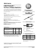

Zener Voltage Regulator
I
F
V
I
I
R
I
ZT
V
R
V
Z
V
F
1N53 Series
http://onsemi.com
2
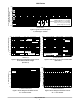
ELECTRICAL CHARACTERISTICS (T
A
= 25°C unless
otherwise noted, V
F
= 1.2 V Max @ I
F
= 1.0 A for all types)
Symbol
Parameter
V
Z
Reverse Zener Voltage @ I
ZT
I
ZT
Reverse Current
Z
ZT
Maximum Zener Impedance @ I
ZT
I
ZK
Reverse Current
Z
ZK
Maximum Zener Impedance @ I
ZK
I
R
Reverse Leakage Current @ V
R
V
R
Breakdown Voltage
I
F
Forward Current
V
F
Forward Voltage @ I
F
I
R
Maximum Surge Current @ T
A
= 25°C
DV
Z
Reverse Zener Voltage Change
I
ZM
Maximum DC Zener Current
ELECTRICAL CHARACTERISTICS (T
A
= 25°C unless otherwise noted, V
F
= 1.2 V Max @ I
F
= 1.0 A for all types)
Device
†
(Note 2)
Device
Marking
Zener Voltage (Note 3) Zener Impedance (Note 3)
Leakage
Current
I
R
(Note 4)
DV
Z
(Note 5)
I
ZM
(Note 6)
V
Z
(Volts) @ I
ZT
Z
ZT
@ I
ZT
Z
ZK
@ I
ZK
I
ZK
I
R
@ V
R
Min Nom Max mA
W W
mA
mA Max
Volts A Volts mA
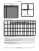
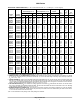
1N5333B 1N5333B 3.14 3.3 3.47 380 3 400 1 300 1 20 0.85 1440
1N5334B 1N5334B 3.42 3.6 3.78 350 2.5 500 1 150 1 18.7 0.8 1320
1N5335B 1N5335B 3.71 3.9 4.10 320 2 500 1 50 1 17.6 0.54 1220
1N5336B 1N5336B 4.09 4.3 4.52 290 2 500 1 10 1 16.4 0.49 1100
1N5337B 1N5337B 4.47 4.7 4.94 260 2 450 1 5 1 15.3 0.44 1010
1N5338B 1N5338B 4.85 5.1 5.36 240 1.5 400 1 1 1 14.4 0.39 930
1N5339B 1N5339B 5.32 5.6 5.88 220 1 400 1 1 2 13.4 0.25 865
1N5340B 1N5340B 5.70 6.0 6.30 200 1 300 1 1 3 12.7 0.19 790
1N5341B 1N5341B 5.89 6.2 6.51 200 1 200 1 1 3 12.4 0.1 765
1N5342B 1N5342B 6.46 6.8 7.14 175 1 200 1 10 5.2 11.5 0.15 700
1N5343B 1N5343B 7.13 7.5 7.88 175 1.5 200 1 10 5.7 10.7 0.15 630
1N5344B 1N5344B 7.79 8.2 8.61 150 1.5 200 1 10 6.2 10 0.2 580
1N5345B 1N5345B 8.27 8.7 9.14 150 2 200 1 10 6.6 9.5 0.2 545
1N5346B 1N5346B 8.65 9.1 9.56 150 2 150 1 7.5 6.9 9.2 0.22 520
1N5347B 1N5347B 9.50 10 10.5 125 2 125 1 5 7.6 8.6 0.22 475
Devices listed in bold, italic are ON Semiconductor Preferred devices. Preferred devices are recommended choices for future use and best overall value.
2. TOLERANCE AND TYPE NUMBER DESIGNATION: The JEDEC type numbers shown indicate a tolerance of ±5%.
3. ZENER VOLTAGE (V
Z
) and IMPEDANCE (I
ZT
and I
ZK
): Test conditions for zener voltage and impedance are as follows: I
Z
is applied
40 ±10 ms prior to reading. Mounting contacts are located 3/8″ to 1/2″ from the inside edge of mounting clips to the body of the diode
(T
A
= 25°C +8°C, −2°C).
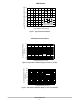
4. SURGE CURRENT (I
R
): Surge current is specified as the maximum allowable peak, non−recurrent square−wave current with a pulse width,
PW, of 8.3 ms. The data given in Figure 5 may be used to find the maximum surge current for a square wave of any pulse width between
1 ms and 1000 ms by plotting the applicable points on logarithmic paper. Examples of this, using the 3.3 V and 200 V zener are shown in
Figure 6. Mounting contact located as specified in Note 2 (T
A
= 25°C +8°C, −2°C).
5. VOLTAGE REGULATION (DV
Z
): The conditions for voltage regulation are as follows: V
Z
measurements are made at 10% and then at 50%
of the I
Z
max value listed in the electrical characteristics table. The test current time duration for each V
Z
measurement is 40 ±10 ms. Mounting
contact located as specified in Note 2 (T
A
= 25°C +8°C, −2°C).
6. MAXIMUM REGULATOR CURRENT (I
ZM
): The maximum current shown is based on the maximum voltage of a 5% type unit, therefore,
it applies only to the B−suffix device. The actual I
ZM
for any device may not exceed the value of 5 watts divided by the actual V
Z
of the device.
T
L
= 25°C at 3/8″ maximum from the device body.
†The “G’’ suffix indicates Pb−Free package or Pb−Free packages are available.