
Data Sheet


2N5551 / MMBT5551 — NPN General-Purpose Amplifier
© 2009 Fairchild Semiconductor Corporation www.fairchildsemi.com
2N5551 / MMBT5551 Rev. 1.1.0 2
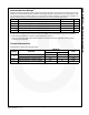
Absolute Maximum Ratings
(2)
Stresses exceeding the absolute maximum ratings may damage the device. The device may not function or be opera-
ble above the recommended operating conditions and stressing the parts to these levels is not recommended. In addi-
tion, extended exposure to stresses above the recommended operating conditions may affect device reliability. The
absolute maximum ratings are stress ratings only. Values are at T
A
= 25°C unless otherwise noted.
Notes:
2. These ratings are limiting values above which the serviceability of any semiconductor device may be impaired.
3. These ratings are based on a maximum junction temperature of 150 °C.
These are steady-state limits. Fairchild Semiconductor should be consulted on applications involving pulsed
or low-duty cycle operations.
Thermal Characteristics
Values are at T
A
= 25°C unless otherwise noted.
Symbol ParameterValueUnits
V
CEO
Collector-Emitter Voltage 160 V
V
CBO
Collector-Base Voltage 180 V
V
EBO
Emitter-Base Voltage 6 V
I
C
Collector current - Continuous 600 mA
T
J
, T
stg
(2)
Junction and Storage Temperature -55 to +150 °C
Symbol Parameter
Maximum
Units
2N5551 MMBT5551
P
D
Total Device Dissipation 625 350 mW
Derate above 25°C5.02.8mW/°C
R
θJC
Thermal Resistance, Junction to Case 83.3 °C/W
R
θJA
Thermal Resistance, Junction to Ambient 200 357 °C/W