
Datasheet


© Semiconductor Components Industries, LLC, 2008
September, 2008 − Rev. 13
1 Publication Order Number:
BD675/D
BD675, BD675A, BD677,
BD677A, BD679, BD679A,
BD681
BD681 is a Preferred Device
Plastic Medium-Power
Silicon NPN Darlingtons
This series of plastic, medium−power silicon NPN Darlington
transistors can be used as output devices in complementary
general−purpose amplifier applications.
Features
• High DC Current Gain:
h
FE
= 750 (Min) @ I
C
= 1.5 and 2.0 Adc
• Monolithic Construction
• BD675, 675A, 677, 677A, 679, 679A, 681 are complementary
with BD676, 676A, 678, 678A, 680, 680A, 682
• BD677, 677A, 679, 679A are equivalent to MJE 800, 801, 802, 803
• Pb−Free Packages are Available*
ÎÎÎÎÎÎÎÎÎÎÎÎÎÎÎÎÎÎÎ
ÎÎÎÎÎÎÎÎÎÎÎÎÎÎÎÎÎÎÎ
MAXIMUM RATINGS
ÎÎÎÎÎÎÎÎÎÎÎ
ÎÎÎÎÎÎÎÎÎÎÎ
Rating
ÎÎÎÎ
ÎÎÎÎ
Symbol
ÎÎÎÎ
ÎÎÎÎ
Value
ÎÎÎ
ÎÎÎ
Unit
ÎÎÎÎÎÎÎÎÎÎÎ
ÎÎÎÎÎÎÎÎÎÎÎ
ÎÎÎÎÎÎÎÎÎÎÎ
ÎÎÎÎÎÎÎÎÎÎÎ
Collector−Emitter Voltage BD675, A
BD677, A
BD679, A
BD681
ÎÎÎÎ
ÎÎÎÎ
ÎÎÎÎ
ÎÎÎÎ
V
CEO
ÎÎÎÎ
ÎÎÎÎ
ÎÎÎÎ
ÎÎÎÎ
45
60
80
100
ÎÎÎ
ÎÎÎ
ÎÎÎ
ÎÎÎ
Vdc
ÎÎÎÎÎÎÎÎÎÎÎ
ÎÎÎÎÎÎÎÎÎÎÎ
ÎÎÎÎÎÎÎÎÎÎÎ
Collector−Base Voltage BD675, A
BD677, A
BD679, A
BD681
ÎÎÎÎ
ÎÎÎÎ
ÎÎÎÎ
V
CBO
ÎÎÎÎ
ÎÎÎÎ
ÎÎÎÎ
45
60
80
100
ÎÎÎ
ÎÎÎ
ÎÎÎ
Vdc
ÎÎÎÎÎÎÎÎÎÎÎ
ÎÎÎÎÎÎÎÎÎÎÎ
Emitter−Base Voltage
ÎÎÎÎ
ÎÎÎÎ
V
EBO
ÎÎÎÎ
ÎÎÎÎ
5.0
ÎÎÎ
ÎÎÎ
Vdc
ÎÎÎÎÎÎÎÎÎÎÎ
ÎÎÎÎÎÎÎÎÎÎÎ
Collector Current
ÎÎÎÎ
ÎÎÎÎ
I
C
ÎÎÎÎ
ÎÎÎÎ
4.0
ÎÎÎ
ÎÎÎ
Adc
ÎÎÎÎÎÎÎÎÎÎÎ
ÎÎÎÎÎÎÎÎÎÎÎ
Base Current
ÎÎÎÎ
ÎÎÎÎ
I
B
ÎÎÎÎ
ÎÎÎÎ
1.0
ÎÎÎ
ÎÎÎ
Adc
ÎÎÎÎÎÎÎÎÎÎÎ
ÎÎÎÎÎÎÎÎÎÎÎ
ÎÎÎÎÎÎÎÎÎÎÎ
Total Device Dissipation @ T
C
= 25°C
Derate above 25°C
ÎÎÎÎ
ÎÎÎÎ
ÎÎÎÎ
P
D
ÎÎÎÎ
ÎÎÎÎ
ÎÎÎÎ
40
0.32
ÎÎÎ
ÎÎÎ
ÎÎÎ
W
W/°C
ÎÎÎÎÎÎÎÎÎÎÎ
ÎÎÎÎÎÎÎÎÎÎÎ
ÎÎÎÎÎÎÎÎÎÎÎ
Operating and Storage Junction
Temperature Range
ÎÎÎÎ
ÎÎÎÎ
ÎÎÎÎ
T
J
, T
stg
ÎÎÎÎ
ÎÎÎÎ
ÎÎÎÎ
– 55 to + 150
ÎÎÎ
ÎÎÎ
ÎÎÎ
°C
ÎÎÎÎÎÎÎÎÎÎÎÎÎÎÎÎÎÎÎ
ÎÎÎÎÎÎÎÎÎÎÎÎÎÎÎÎÎÎÎ
THERMAL CHARACTERISTICS
ÎÎÎÎÎÎÎÎÎÎÎ
ÎÎÎÎÎÎÎÎÎÎÎ
Characteristic
ÎÎÎÎ
ÎÎÎÎ
Symbol
ÎÎÎÎ
ÎÎÎÎ
Max
ÎÎÎ
ÎÎÎ
Unit
ÎÎÎÎÎÎÎÎÎÎÎ
ÎÎÎÎÎÎÎÎÎÎÎ
Thermal Resistance,
Junction−to−Case
ÎÎÎÎ
ÎÎÎÎ
q
JC
ÎÎÎÎ
ÎÎÎÎ
3.13
ÎÎÎ
ÎÎÎ
°C/W
Maximum ratings are those values beyond which device damage can occur.
Maximum ratings applied to the device are individual stress limit values (not
normal operating conditions) and are not valid simultaneously. If these limits are
exceeded, device functional operation is not implied, damage may occur and
reliability may be affected.
*For additional information on our Pb−Free strategy and soldering details, please
download the ON Semiconductor Soldering and Mounting Techniques
Reference Manual, SOLDERRM/D.
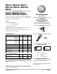
http://onsemi.com
4.0 AMPERES
POWER TRANSISTORS
NPN SILICON
60, 80, 100 VOLTS, 40 WATTS
TO−225AA
CASE 77
STYLE 1
MARKING DIAGRAMS
YWW
BD6xxG
3
2
1
Preferred devices are recommended choices for future use
and best overall value.
See detailed ordering and shipping information in the package
dimensions section on page 4 of this data sheet.
ORDERING INFORMATION
BD6xx = Device Code
x = 75, 77, 79, 81
Y = Year
WW = Work Week
G=Pb−Free Package
YWW
B
BD6xxAG
COLLECTOR 2
BASE
3
EMITTER 1