
Data Sheet

2005 Semiconductor Components Industries, LLC.
September-2017, Rev. 3
Publication Order Number:
BSS138/D
BSS138
N-Channel Logic Level Enhancement Mode Field Effect Transistor
General Description
These N-Channel enhancement mode field
effect transistors are produced using ON
Semicondcutor
’s proprietary, high cell density, DMOS
technology. These products have been designed to
minimize on-state resistance while provide rugged,
reliable, and fast switching performance.These
products are particularly suited for low voltage, low
current applications such as small servo motor
control, power MOSFET gate drivers, and other
switching applications.
Features
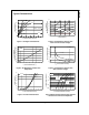
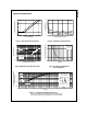
• 0.22 A, 50 V. R
DS(ON)
= 3.5Ω @ V
GS
= 10 V
R
DS(ON)
= 6.0Ω @ V
GS
= 4.5 V
• High density cell design for extremely low R
DS(ON)
• Rugged and Reliable
• Compact industry standard SOT-23 surface mount
package
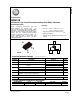
G
D
S
SOT-23
D
S
G
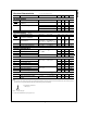
Absolute Maximum Ratings T
A
=25
o
C unless otherwise noted
Symbol Parameter Ratings Units
V
DSS
Drain-Source Voltage 50 V
V
GSS
Gate-Source Voltage
±20
V
I
D
Drain Current – Continuous (Note 1) 0.22 A
– Pulsed 0.88
Maximum Power Dissipation (Note 1) 0.36
W
P
D
Derate Above 25°C
2.8
mW/°C
T
J
, T
STG
Operating and Storage Junction Temperature Range
−55 to +150 °C
T
L
Maximum Lead Temperature for Soldering
Purposes, 1/16” from Case for 10 Seconds
300
°C
Thermal Characteristics
R
θJA
Thermal Resistance, Junction-to-Ambient
(Note 1) 350
°C/W
Package Marking and Ordering Information
Device Marking Device Reel Size Tape width Quantity
SS BSS138 7’’ 8mm 3000 units
BSS138