
Data Sheet

www.onsemi.com
10
FAN7085-GF085 High Side Gate Driver with Recharge FET
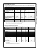
Performance Graphs
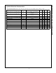
4.4 4.7 5.0 5.3 5.6 5.9 6.2 6.5
2.2
2.4
2.6
2.8
3.0
3.2
Typ.
Vinth+ (V)
Vsupply (V)
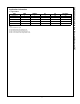
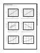
Figure 5a. Positive IN and RESET Threshold vs VCC Supply Figure 5b. Negative IN and RESET Threshold vs VCC Supply
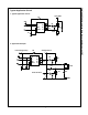
Figure6b. Output Source Current vs Temperature
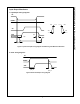
Figure 7a. Turn-On Propagation Delay Time vs Temperature
Figure 7b. Turn-Off Propagation Delay Time vs Temperature
Figure6a. Output Sink Current vs VBS Supply
VBS=7V, RL=50, CL=2.5nF
4.4 4.7 5.0 5.3 5.6 5.9 6.2 6.5
1.8
2.0
2.2
2.4
2.6
Typ.
Vinth- (V)
Vsupply (V)
5101520
0
400
800
1200
1600
2000
125
o
C
Output Sink Cureent (mA)
VBS(V)
-40
o
C
-50 0 50 100 150
300
350
400
450
500
Typ.
Output Source Cureent (mA)
Temperature (
o
C)
-50 0 50 100 150
500
530
560
590
620
650
Turn-on Propagation Delay (ns)
Temperature(
o
C)
Typ.
-50 0 50 100 150
100
150
200
250
Turn-off Propagation Delay (ns)
Temperature (
o
C)
Typ.
VBS=7V, RL=50, CL=2.5nF
VCC=5V, VBS=7VVCC=5V
VCC=5V,VBS=7V, RL=50, CL=2.5nFVCC=5V,VBS=7V, RL=50, CL=2.5nF
This performance graphs based on ambient temperature -40C ~125C