
Data Sheet
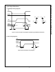
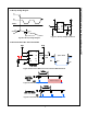


Figure 12a. VCC Under Voltage Threshold(+) vs Temperature
Figure 12b. VCC Under Voltage Threshold(-) vs Temperature
Figure 13. Recharge FET Turn-on Delay time
Figure 15. Recharge FET I-V curve
Figure 14. Recharge FET Turn-off Delay time
VBS=7V
-50 0 50 100 150
2.0
2.5
3.0
3.5
4.0
4.5
5.0
V
CC
Supply Voltage(V)
Temperature(
o
C)
Max.
Typ.
Min.
-50 0 50 100 150
2.0
2.5
3.0
3.5
4.0
4.5
5.0
V
CC
Supply Voltage(V)
Temperature(
o
C)
Max.
Typ.
Min.
-50 0 50 100 150
4
6
8
10
Typ.
Recharge Transistor Turn-on Propagation
Delay (us)
Temperature(
o
C)
-50 0 50 100 150
140
180
220
260
300
Typ.
Recharge Gate Turn-off Propagation
Delay (ns)
Temperature (
o
C)
0.4 0.6 0.8 1.0 1.2
0.2
0.6
1.0
1.4
1.8
I (mA)
V (V)
Typ.
-50 0 50 100 150
4
6
8
10
Typ.
High Side Turn-off to Recharge Gate
Turn-on (us)
Temperature (
o
C)
Figure 16. High Side Turn-off to Recharge FET turn-on VS Temperature
VCC=5v, VBS=7, VRL=50, CL=2.5nF VCC=5v, VBS=7V, RL=50, CL=2.5nF
VCC=5v, VBS=7V, RL=50, CL=2.5nF VCC=5v, VBS=7V, RL=50, CL=2.5nF
www.onsemi.com
12
FAN7085-GF085 High Side Gate Driver with Recharge FET