
Data Sheet

www.onsemi.com
2
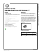
FAN7085-GF085 High Side Gate Driver with Recharge FET
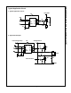
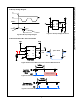
Block Diagrams
VCC
Under Voltage
Reset VCC to GND
Logic
Pulse
Filter
Level Shifter
ON
Level Shifter
OFF
Delay
Under
Voltage Reset
VB to VS
Pulse Filter
Flip Flop
Brake before
make
RESET-
IN-
GND
VS
HO
VB
Recharge Path
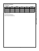
Pin Assignments
1
2
3
4
5
6
7
8
VCC
IN
GND
RESET
VS
NC
HO
VB
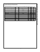
Pin Definitions
Pin Number Pin Name I/O Pin Function Description
1 VCC P Driver supply voltage, typically 5V
2 IN- I Driver control signal input (Negative Logic)
3 GND P Ground
4 RESET- I Driver enable input signal (Negative Logic)
5 VS P High side floating offset for
MOSFET Sour
ce connection
6 NC - No connection (No Bond wire)
7 HO A High side drive output for MOSFET Gate connection
8 VB P Driver output stage supply