
Data Sheet

www.onsemi.com
3
FAN7085-GF085 High Side Gate Driver with Recharge FET
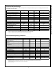
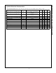
Absolute Maximum Ratings
Absolute Maximum Ratings indicate sustained limits beyond which damage to the device may occur. All voltage parameters are abso-
lute voltages referenced to GND.
Parameter Symbol Min. Max. Unit
High side floating supply voltage VBS -0.3 25 V
High side driver output stage voltage
Neg. transient: 0.5 ms, external MOSFET off
VB -5 325 V
High side floating supply offset voltage
Neg. transient 0.2 us
Vs -25 300 V
High side floating output voltage V
HO VS-0.3 VB+0.3 V
Supply voltage V
CC -0.3 25 V
Input voltage for IN- V
IN -0.3 Vcc+0.3 V
Input voltage for RESET- V
RES -0.3 Vcc+0.3 V
Power Dissipation
1)
Pd 0.625 W
Thermal resistance, junction to ambient
1)
Rthja 200 C/W
Electrostatic discharge voltage
(Human Body Model)
V
ESD
1.5K V
Charge device model V
CDM
500 V
Junction Temperature Tj 150 C
Storage Temperature T
S
-55 150 C
Note: 1) The thermal resistance and power dissipation rating are measured bellow conditions;
JESD51-2: Integrated Circuit Thermal Test Method Environmental Conditions - Natural condition(StillAir)
JESD51-3: Low Effective Thermal Conductivity Test Board for Leaded Surface Mount Package
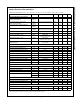
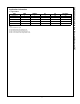
Recommended Operating Conditions
For proper operation the device should be used within the recommended conditions
Parameter Symbol Min. Max. Unit
High side floating supply voltage(DC)
Transient:-10V@ 0.2 us
VB VS+4.5 VS+20 V
High side floating supply offset voltage(DC)
@VBS=7V
VS -3 300 V
High side floating supply offset voltage(Transient)
0.2us @VBS<25V
VS -25 300 V
High side floating output voltage V
HO Vs VB V
Allowable offset voltage Slew Rate
1)
dv/dt - 50 V/ns
Supply voltage for logic part V
CC 4.5 20 V
Input voltage for IN-
VIN 0 Vcc V
Input voltage for RESET- V
RESET 0 Vcc V
Switching frequency
2)
Fs 200K Hz
Minimum low input width
3)
tIN(low,min) 560 - ns
Minimum high input width
3)
tIN(high,min) 60 - ns
Minimum operating voltage of VB related to GND V
B(MIN)
4)
4 - V
Ambient temperature T
a -40 125 C
.-40°C <= Ta
<= 125°C
Note: 1) Guaranteed by design.
2) Duty = 0.5, VBS >=7V
3) Guaranteed by design. Pulse widths below the specified values, may be ignored. Output will either follow the input signal or
will ignore it.
No false output state is guaranteed when minimum input width is smaller than tin
4) Guaranteed by design