
Data Sheet

www.onsemi.com
4
FAN7085-GF085 High Side Gate Driver with Recharge FET
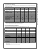
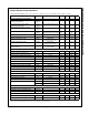
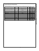
Statics Electrical Characteristics
Unless otherwise specified, -40°C <= Ta <= 125°C, VCC = 5V, VBS = 7V, VS = 0V, VRESET = 5V, RL = 50, CL = 2.5nF.
Parameter Symbol Conditions Min. Typ. Max. Unit
VCC and VBS Supply Characteristics
V
CC and VBS supply under voltage
positive going threshold
VCCUV+
VBSUV+
Vcc and VBS rising from 0V - 3.7 4.3 V
V
CC and VBS supply under voltage
negative going threshold
VCCUV-
V
BSUV-
Vcc and VBS dropping from 5V 2.8 3.4 - V
V
CC and VBS under voltage hysteresis VCCUVH
VBSUVH
- 0.02 0.3 - V
Under voltage lockout response time tduvcc
tduvbs
VCC: 6.5V->2.4V or 2.4V->6.5V
VBS: 6.5V->2.4V or 2.4V->6.5V
0.5
0.5
20
20
us
us
Offset supply leakage current I
LK VB=VS=300V - - 200 uA
Quiescent Vcc supply current I
QCC Vcc=20V - - 500 uA
Quiescent VBS supply current I
QBS1 Static mode,
V
BS=7V, VIN=0 or 5V
100 uA
Quiescent VBS supply current I
QBS2 Static mode,
V
BS=16V, VIN=0 or 5V
200 uA
VBS drop due to output turn-on
(Design guaranty)
V
BS VBS=7V, Cbs=1uF, tdIG-IN =3uS,
t
TEST=100uS
210 mV
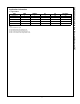
Input Characteristics
High logic level input voltage for IN- V
IH 0.6VCC - - V
Low logic level input voltage for IN- V
IL - - 0.28VCC V
Low logic level input bias current for IN- I
IN- VIN=0 5 25 60 uA
High logic level input bias current for IN- I
IN+ VIN=5V - - 5 uA
Full up resistance at IN R
IN 83 200 1000
High logic level input voltage for RESET- V
RH 0.6Vcc - - V
Low logic level input voltage for RESET- V
RL 0.28Vcc V
High logic level input current for RESET- I
RES+ VRESET=5V 5 25 60 uA
Low logic level input bias current for RESET- I
RES- VRESET=0 5 uA
Full down resistance at RESET- R
RES 83 200 1000
Output characteristics
High level output voltage, V
B - VHO VOH IO=0 - - 0.1 V
Low level output voltage, VHO-GND V
OL IO=0 - - 0.1 V
Peak output source current I
O+ VIN=5V 250 450 - mA
Peak output sink current I
O- VIN=0 250 450 - mA
Equivalent output resistance R
OP 15.5 28
R
ON 15.5 28
Recharge Characteristics
Recharge TR turn-on propagation delay T
on_rech 4 7.9 9.8 us
Recharge TR turn-off propagation delay T
off_rech 0.2 0.4 us
Recharge TR on-state voltage drop V
RECH Is=1mA, VIN=5V @125C 1.2 V
Dead Time Characteristics
High side turn-off to recharge gate turn-on D
THOFF Vcc=5V, VS=7V 4 7.8 9.8 us
Recharge gate turn-off to high side turn-on D
THON Vcc=5V, VS=7V 0.1 0.4 0.7 us
Note: The input parameter are referenced to GND. The VO and IO parameters are referenced to GND.