
Data Sheet

www.onsemi.com
9
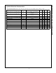
FAN7085-GF085 High Side Gate Driver with Recharge FET
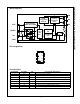
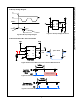
3.VB Drop Voltage Diagram
VBdrop
IN-
RESET-
VB-VS
I
g
7V
Brake before make
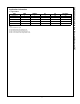
VCC
IN-
GND
RESET-
VB
HO
NC
VS
1u
50R
2n5
Ig
Figure3.b VB Drop Voltage Test Circuit
Figure3.a VB Drop Voltage Diagram
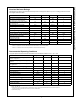
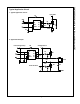
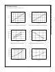
4.Recommendation Min. Short Pulse Width
Figure 4a.Short Pulse Width Test Circuit and Pulse Width Waveform
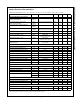
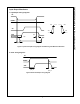
Figure 4b. Abnormal Output Waveform with short pulse width
Figure 4c. Recommendation of pulse width Output Waveform
Bat1
1
2
4
5
6
7
8
3
VCC
IN
RESET
N.C
VS
HO
VB
COM
Bat2
0.1uF
FAN7085
IN
60%
28%
Tpulse =560nS
Less than
430nS Pulse
Width
142KHz
IN
HO
Abnormal Output
Recommended
pulse width 560nS
142KHz
HO
IN