
Data Sheet


FDG8842CZ Complementary PowerTrench
®
MOSFET
©2007 Semic
onductor Components Industries, LLC.
October-2017, Rev.2
Public
ation Order Number:
FDG8842CZ/D
1
FDG8842CZ
Complementary PowerTrench
®
MOSFET
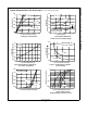
Q1:30V,0.75A,0.4Ω; Q2:–25V,–0.41A,1.1Ω
Features
Q1: N-Channel
Max r
DS(on)
= 0.4Ω at V
GS
= 4.5V, I
D
= 0.75A
Max r
DS(on)
= 0.5Ω at V
GS
= 2.7V, I
D
= 0.67A
Q2: P-Channel
Max r
DS(on)
= 1.1Ω at V
GS
= –4.5V, I
D
= –0.41A
Max r
DS(on)
= 1.5Ω at V
GS
= –2.7V, I
D
= –0.25A
Very low level gate drive requirements allowing direct
operation in 3V circuits(V
GS(th)
<1.5V)
Very small package outline SC70-6
RoHS Compliant
General Description
These N & P-Channel logic level enhancement mode field
effect transistors are produced using ON Semiconductor’s
proprietary, high cell density, DMOS technology. This very
high density process is especially tailored to minimize
on-state resistance. This device has been designed
especially for low voltage applica-tions as a replacement for
bipolar digital transistors and small signal MOSFETs. Since
bias resistors are not required, this dual digital FET can replace
several different digital transistors, with different bias resistor
values.
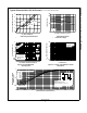
MOSFET Maximum Ratings T
A
= 25°C unless otherwise noted
Thermal Characteristics
Package Marking and Ordering Information
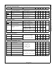
Symbol Parameter Q1 Q2 Units
V
DS
Drain to Source Voltage 30 –25 V
V
GS
Gate to Source Voltage ±12 –8 V
I
D
Drain Current -Continuous 0.75 –0.41
A
-Pulsed
2.2 –1.2
P
D
Power Dissipation for Single Operation (Note 1a)
(Note 1b)
0.36
W
0.30
T
J
, T
STG
Operating and Storage Junction Temperature Range –55 to +150 °C
R
θJA
Thermal Resistance, Junction to Ambient Single operation (Note 1a) 350
°C/W
R
θJA
Thermal Resistance, Junction to Ambient Single operation (Note 1b) 415
Device Marking Device Reel Size Tape Width Quantity
.42 FDG8842CZ 7” 8mm 3000 units
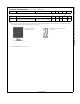
S1
G1
D2
D1
G2
S2
S1
S2
G2
D1
D2
G1
Pin 1
SC70-6
Q1
Q2