
Data Sheet


FDG8842CZ Complementary PowerTrench
®
MOSFET
www.onsemi.com
3
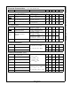
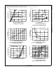
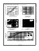
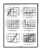
Electrical Characteristics T
J
= 25°C unless otherwise noted
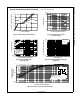
Drain-Source Diode Characteristics and Maximum Ratings
Symbol Parameter Test Conditions Type Min Typ Max Units
I
S
Maximum Continuous Drain-Source Diode Forward Current
Q1
Q2
0.3
–0.3
A
V
SD
Source to Drain Diode Forward Voltage
V
GS
= 0V, I
S
= 0.3A (Note 2)
V
GS
= 0V, I
S
= –0.3A (Note 2)
Q1
Q2
0.76
–0.84
1.2
–1.2
V
Notes:
1. R
θJA
is the sum of the junction-to-case and case-to-ambient thermal resistance where the case thermal reference is defined as the solder mounting surface of the drain pins.
R
θJC
is guaranteed by design while R
θJA
is determined by the user's board design.
2. Pulse Test: Pulse Width < 300μs, Duty cycle < 2.0%.
a. 350°C/W when mounted on a
1 in
2
pad of 2 oz copper .
b. 415°C/W when mounted on a minimum pad
of 2 oz copper.
Scale 1:1 on letter size paper.