
Data Sheet


© 2011 Fairchild Semiconductor Corporation www.fairchildsemi.com
FDMF6823A • Rev. 1.0.3 13
FDMF6823A — Extra-Small, High-Performance, High-Frequency DrMOS Module
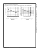
Adaptive Gate Drive Circuit
The driver IC advanced design ensures minimum
MOSFET dead-time, while eliminating potential shoot-
through (cross-conduction) currents. It senses the state
of the MOSFETs and adjusts the gate drive adaptively
to ensure they do not conduct simultaneously. Figure 27
provides the relevant timing waveforms. To prevent
overlap during the LOW-to-HIGH switching transition
(Q2 off to Q1 on), the adaptive circuitry monitors the
voltage at the GL pin. When the PWM signal goes
HIGH, Q2 begins to turn off after a propagation delay
(t
PD_PHGLL
). Once the GL pin is discharged below 1.0 V,
Q1 begins to turn on after adaptive delay t
D_DEADON
.
To preclude overlap during the HIGH-to-LOW transition
(Q1 off to Q2 on), the adaptive circuitry monitors the
voltage at the GH-to-PHASE pin pair. When the PWM
signal goes LOW, Q1 begins to turn off after a
propagation delay (t
PD_PLGHL
). Once the voltage across
GH-to-PHASE falls below 2.2 V, Q2 begins to turn on
after adaptive delay t
D_DEADOFF
.
Figure 27. PWM and 3-StateTiming Diagram
t
PD_TSGHH
V
SWH
GH
to
V
SWH
GL
t
PD_PHGLL
t
D_HOLD-OFF
90%
Exit
3-state
1.0
V
PWM
V
IL_PWM
V
IH_PWM
V
TRI_HI
V
IH_PWM
V
IH_PWM
10%
t
R_GL
t
D_HOLD-OFF
Exit
3-state
V
IH_PWM
V
TRI_HI
V
TRI_LO
V
IL_PWM
t
PD_PLGHL
t
PD_TSGHH
DCM
t
F_GH
t
R_GH
t
D_HOLD-OFF
10%
CCM
DCM
Exit
3-state
90%
10%
90%
Enter
3-state
Enter
3-state
t
D_DEADOFF
t
D_DEADON
Enter
3-state
t
F_GL
V
IN
V
OUT
2.2V
t
PD_TSGLH
Notes:
t
PD_xxx
= propagation delay from external signal (PWM, SMOD#, etc.) to IC generated signal. Example (t
PD_PHGLL
– PWM going HIGH to LS V
GS
(GL) going LOW)
t
D_xxx
= delay from IC generated signal to IC generated signal. Example (t
D_DEADON
– LS V
GS
(GL) LOW to HS V
GS
(GH) HIGH)
PWM
Exiting 3-state
t
PD_PHGLL
= PWM rise to LS V
GS
fall, V
IH_PWM
to 90% LS V
GS
t
PD_TSGHH
= PWM 3-state to HIGH to HS V
GS
rise, V
IH_PWM
to 10% HS V
GS
t
PD_PLGHL
= PWM fall to HS V
GS
fall, V
IL_PWM
to 90% HS V
GS
t
PD_TSGLH
= PWM 3-state to LOW to LS V
GS
rise, V
IL_PWM
to 10% LS V
GS
t
PD_PHGHH
= PWM rise to HS V
GS
rise, V
IH_PWM
to 10% HS V
GS
(SMOD# held LOW)
SMOD# Dead Times
t
PD_SLGLL
= SMOD# fall to LS V
GS
fall, V
IL_SMOD
to 90% LS V
GS
t
D_DEADON
= LS V
GS
fall to HS V
GS
rise, LS-comp trip value (~1.0V GL) to 10% HS V
GS
t
PD_SHGLH
= SMOD# rise to LS V
GS
rise, V
IH_SMOD
to 10% LS V
GS
t
D_DEADOFF
= VSWH fall to LS V
GS
rise, SW-comp trip value (~2.2V VSWH) to 10% LS V
GS