
Data Sheet
© 2011 Fairchild Semiconductor Corporation www.fairchildsemi.com
FDMF6823A • Rev. 1.0.3 6
FDMF6823A — Extra-Small, High-Performance, High-Frequency DrMOS Module
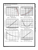
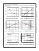
Electrical Characteristics
Typical values are V
IN
= 12 V, V
CIN
= 5 V, V
DRV
= 5 V, and T
A
= T
J
= +25°C unless otherwise noted.
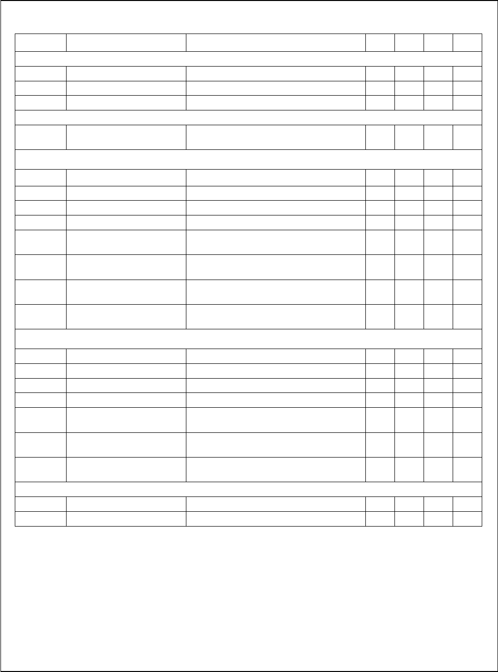
Symbol Parameter Condition Min. Typ. Max. Unit
Thermal Warning Flag
T
ACT
Activation Temperature 150 °C
T
RST
Reset Temperature 135 °C
R
THWN
Pull-Down Resistance
I
PLD
=5 mA
30 Ω
250 ns Timeout Circuit
t
D_TIMEOUT
Timeout Delay
SW=0 V, Delay Between GH from HIGH to
LOW and GL from LOW to HIGH
250 ns
High-Side Driver (f
SW
= 1000 kHz, I
OUT
= 30 A, T
A
= +25°C)
R
SOURCE_GH
Output Impedance, Sourcing
Source Current=100 mA
1 Ω
R
SINK_GH
Output Impedance, Sinking
Sink Current=100 mA
0.8 Ω
t
R_GH
Rise Time GH=10% to 90% 10 ns
t
F_GH
Fall Time GH=90% to 10% 10 ns
t
D_DEADON
LS to HS Deadband Time
GL Going LOW to GH Going HIGH,
1.0 V GL to 10% GH
15 ns
t
PD_PLGHL
PWM LOW Propagation
Delay
PWM Going LOW to GH Going LOW,
V
IL_PWM
to 90% GH
20 30 ns
t
PD_PHGHH
PWM HIGH Propagation
Delay (SMOD# =0)
PWM Going HIGH to GH Going HIGH,
V
IH_PWM
to 10% GH (SMOD# =0, I
D_LS
>0)
30 ns
t
PD_TSGHH
Exiting 3-State Propagation
Delay
PWM (From 3-State) Going HIGH to GH
Going HIGH, V
IH_PWM
to 10% GH
30 ns
Low-Side Driver (f
SW
= 1000 kHz, I
OUT
= 30 A, T
A
= +25°C)
R
SOURCE_GL
Output Impedance, Sourcing
Source Current=100 mA
1 Ω
R
SINK_GL
Output Impedance, Sinking
Sink Current=100 mA
0.5 Ω
t
R_GL
Rise Time GL=10% to 90% 30 ns
t
F_GL
Fall Time GL=90% to 10% 15 ns
t
D_DEADOFF
HS to LS Deadband Time
SW Going LOW to GL Going HIGH,
2.2 V SW to 10% GL
15 ns
t
PD_PHGLL
PWM-HIGH Propagation
Delay
PWM Going HIGH to GL Going LOW,
V
IH_PWM
to 90% GL
10 25 ns
t
PD_TSGLH
Exiting 3-State Propagation
Delay
PWM (From 3-State) Going LOW to GL
Going HIGH, V
IL_PWM
to 10% GL
20 ns
Boot Diode
V
F
Forward-Voltage Drop
I
F
=20 mA
0.3 V
V
R
Breakdown Voltage
I
R
=1 mA
22 V