
Data Sheet

JFET Chopper Transistors
N–Channel — Depletion
MAXIMUM RATINGS
Rating Symbol Value Unit
Drain–Gate Voltage V
DG
–35 Vdc
Gate–Source Voltage V
GS
–35 Vdc
Gate Current I
G
50 mAdc
Total Device Dissipation @ T
A
= 25°C
Derate above 25°C
P
D
350
2.8
mW
mW/°C
Lead Temperature T
L
300 °C
Operating and Storage Junction
Temperature Range
T
J
, T
stg
–65 to +150 °C
ELECTRICAL CHARACTERISTICS (T
A
= 25°C unless otherwise noted)
Characteristic
Symbol Min Max Unit
OFF CHARACTERISTICS
Gate–Source Breakdown Voltage
(I
G
= –1.0 µAdc)
V
(BR)GSS
35 — Vdc
Gate Reverse Current
(V
GS
= –15 Vdc)
I
GSS
— –1.0 nAdc
Gate Source Cutoff Voltage
(V
DS
= 5.0 Vdc, I
D
= 1.0 µAdc) J111
J112
J113
V
GS(off)
–3.0
–1.0
–0.5
–10
–5.0
–3.0
Vdc
Drain–Cutoff Current
(V
DS
= 5.0 Vdc, V
GS
= –10 Vdc)
I
D(off)
— 1.0 nAdc
ON CHARACTERISTICS
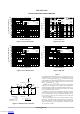
Zero–Gate–Voltage Drain Current
(1)
(V
DS
= 15 Vdc) J111
J112
J113
I
DSS
20
5.0
2.0
—
—
—
mAdc
Static Drain–Source On Resistance
(V
DS
= 0.1 Vdc) J111
J112
J113
r
DS(on)
—
—
—
30
50
100
Ω
Drain Gate and Source Gate On–Capacitance
(V
DS
= V
GS
= 0, f = 1.0 MHz)
C
dg(on)
+
C
sg(on)
— 28 pF
Drain Gate Off–Capacitance
(V
GS
= –10 Vdc, f = 1.0 MHz)
C
dg(off)
— 5.0 pF
Source Gate Off–Capacitance
(V
GS
= –10 Vdc, f = 1.0 MHz)
C
sg(off)
— 5.0 pF
1. Pulse Width = 300 µs, Duty Cycle = 3.0%.
ON Semiconductor
Semiconductor Components Industries, LLC, 2001
June, 2001 – Rev. 1
1 Publication Order Number:
J111/D
J111
J112
J113
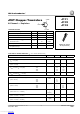
CASE 29–11, STYLE 5
TO–92 (TO–226AA)
1
2
3
1 DRAIN
2 SOURCE
3
GATE
Downloaded from Arrow.com.