
Data Sheet


KA3842B/KA3843B/KA3844B/KA3845B
4
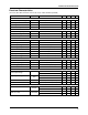
Electrical Characteristics
(Continued)
(V
CC
=15V, R
T
=10KΩ, C
T
=3.3nF, T
A
= 0°C to +70°C unless otherwise specified)
Adjust V
CC
above the start threshould before setting at 15V
Note:
1. Parameter measured at trip point of latch
2. Gain defined as:
3. These parameters, although guaranteed, are not 100 tested in production.
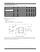
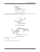
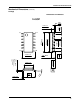
Figure 1. Open Loop Test Circuit
High peak currents associated with capacitive loads necessitate careful grounding techniques Timing and bypass capacitors
should be connected close to pin 5 in a single point ground. The transistor and 5KΩ potentiometer are used to sample the
oscillator waveform and apply an adjustable ramp to pin 3.
Parameter Symbol Conditions Min. Typ. Max. Unit
PWM SECTION
Max. Duty Cycle
D
(Max)
KA3842B/KA3843B 95 97 100 %
D
(MAX)
KA3844B/KA3845B 47 48 50 %
Min. Duty Cycle D
(MIN)
- --0%
TOTAL STANDBY CURRENT
Start-Up Current I
ST
- -0.451mA
Operating Supply Current I
CC(OPR)
V
pin3
=V
pin2
=ON - 14 17 mA
Zener Voltage V
Z
I
CC
= 25mA 30 38 - V
A
∆V
pin1
∆V
pin3
------------------=
,0 ≤ V
pin3
≤ 0.8V