
Data Sheet

KA78RM33R — Low Dropout Voltage Regulator
© 2002 Fairchild Semiconductor Corporation www.fairchildsemi.com
KA78RM33R Rev. 1.1.2 3
Absolute Maximum Ratings
Stresses exceeding the absolute maximum ratings may damage the device. The device may not function or be opera-
ble above the recommended operating conditions and stressing the parts to these levels is not recommended. In addi-
tion, extended exposure to stresses above the recommended operating conditions may affect device reliability. The
absolute maximum ratings are stress ratings only. Values are at T
A
= 25°C unless otherwise noted.
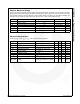
Electrical Characteristics
Values are at T
A
= 25°C, V
IN
= 5 V, I
O
= 0.25 A unless otherwise specified.
Symbol Parameter Value Remark Unit
V
IN
Input Voltage 20 V
I
O
Output Current 0.5 A
R
θJA
Thermal Resistance Junction-Air 110 No Heatsink °C/W
P
D
Power Dissipation Internally limited
T
J
Junction Temperature 150 °C
T
OPR
Operating Temperature -40 to +125 °C
Symbol Parameter Conditions Min. Typ. Max. Unit
V
OUT
Output Voltage I
O
=10 mA 3.22 3.30 3.38 V
R
LOAD
Load Regulation 5 mA < I
O
< 0.5 A 2.0 20 mV
R
LINE
Line Regulation 4.3 V < V
IN
< 16 V 2.0 20 mV
R
R
Ripple Rejection Ratio f = 120 Hz, V
IN
=5 V ± 0.5 V
RMS
55 dB
V
DROP
Dropout Voltage I
O
= 0.5 A 0.6 V
I
Q
Quiescent Current I
O
= 0 A 5.0 10 mA
I
PK
Peak Current V
IN
= 5 V 0.5 1.0 A
V
N
Output Noise Voltage 10 Hz < f < 100 kHz 50 μV
RMS
ΔV
OUT
/ΔT
Temperature Coefficient of Output
Voltage
-40°C < T
J
< 125°C, I
O
= 100 mA -0.2 mV /°C