
Datasheet


Semiconductor Components Industries, LLC, 2004
August, 2004 − Rev. 12
1 Publication Order Number:
LM317M/D
LM317M
500 mA Adjustable Output,
Positive Voltage Regulator
The LM317M is an adjustable three−terminal positive voltage
regulator capable of supplying in excess of 500 mA over an output
voltage range of 1.2 V to 37 V. This voltage regulator is exceptionally
easy to use and requires only two external resistors to set the output
voltage. Further, it employs internal current limiting, thermal
shutdown and safe area compensation, making it essentially blow−out
proof.
The LM317M serves a wide variety of applications including local,
on−card regulation. This device also makes an especially simple
adjustable switching regulator, a programmable output regulator, or by
connecting a fixed resistor between the adjustment and output, the
LM317M can be used as a precision current regulator.
Features
• Output Current in Excess of 500 mA
• Output Adjustable between 1.2 V and 37 V
• Internal Thermal Overload Protection
• Internal Short Circuit Current Limiting
• Output Transistor Safe−Area Compensation
• Floating Operation for High Voltage Applications
• Eliminates Stocking Many Fixed Voltages
• Pb−Free Packages are Available
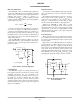
Figure 1. Simplified Application
* = C
in
is required if regulator is located an appreciable distance from power supply filter.
** = C
O
is not needed for stability, however, it does improve transient response.
Since I
Adj
is controlled to less than 100 A, the error associated with this
term is negligible in most applications.
LM317M
V
in
V
out
R
1
240
R
2
Adjust
I
Adj
*
C
in
0.1F
**
+
C
O
1.0F
V
in
V
out
V
out
1.25 V
1
R
2
R
1
I
Adj
R
2
TO−220AB
T SUFFIX
CASE 221A
1
2
3
PIN ASSIGNMENT
1
2
3V
in
Adjust
V
out
ORDERING INFORMATION
See detailed ordering and shipping information in the package
dimensions section on page 12 of this data sheet.
1
2
3
Heatsink Surface (shown as terminal 4 in
case outline drawing) is connected to Pin 2.
SOT−223
ST SUFFIX
CASE 318E
DPAK
DT SUFFIX
CASE 369C
Heatsink surface
connected to Pin 2
http://onsemi.com
1
2
3
4
See general marking information in the device marking
section on page 13 of this data sheet.
DEVICE MARKING INFORMATION
http://onsemi.com