MC7800, MC7800A, MC7800AE, NCV7800 1.0 A Positive Voltage Regulators These voltage regulators are monolithic integrated circuits designed as fixed-voltage regulators for a wide variety of applications including local, on-card regulation. These regulators employ internal current limiting, thermal shutdown, and safe-area compensation. With adequate heatsinking they can deliver output currents in excess of 1.0 A.
MC7800, MC7800A, MC7800AE, NCV7800 Vin MC7800 R24 50 D2 Zener LAT 3 A Q18 LAT Q17 Q19 QNPN C3 R19 27.5 k Q20 QNPN 1.0 P R14 1.0 k Q10 QNPN R18 100 k R21 600 R22 100 Q7 QNPN R15 680 R23 0.2 Vout 5.01 Q5 QNPN 2 R17 9.0 k R11 15 k Q6 QNPN D1 Zener R30 18 k Q12 QNPN Q9 QNPN 2 Q15 QNPN R1 10.66 k R16 600 R20 17500 Q8 QNPN R2 1.56 k Q1 C2 3.0 P R10 3340-(3316ACT) R9 3.0 k R5 4.5 k Q14 QNPN Sense N+ QNPN 6 SUB Q11 2 C1 30 P Q4 QNPN Q13 QNPN Q3 QNPN Q2 Q16 QNPN 4 Diode R6 1.
MC7800, MC7800A, MC7800AE, NCV7800 ELECTRICAL CHARACTERISTICS (Vin = 10 V, IO = 500 mA, TJ = Tlow to 125°C (Note 1), unless otherwise noted) MC7805B, NCV7805 MC7805C Symbol Min Typ Max Min Typ Max Unit Output Voltage (TJ = 25°C) VO 4.8 5.0 5.2 4.8 5.0 5.2 Vdc Output Voltage (5.0 mA ≤ IO ≤ 1.0 A, PD ≤ 15 W) 7.0 Vdc ≤ Vin ≤ 20 Vdc 8.0 Vdc ≤ Vin ≤ 20 Vdc VO 4.75 5.0 5.25 4.75 - 5.0 - 5.25 - 5.0 1.3 100 50 - 0.5 0.8 20 10 - 1.3 0.15 100 50 - 1.3 1.3 25 25 - 3.2 8.0 - 3.
MC7800, MC7800A, MC7800AE, NCV7800 ELECTRICAL CHARACTERISTICS (Vin = 10 V, IO = 1.0 A, TJ = Tlow to 125°C (Note 3), unless otherwise noted) MC7805AB/MC7805AC/NCV7805AB Characteristic Symbol Min Typ Max Unit Output Voltage (TJ = 25°C) VO 4.9 5.0 5.1 Vdc Output Voltage (5.0 mA ≤ IO ≤ 1.0 A, PD ≤ 15 W) 7.5 Vdc ≤ Vin ≤ 20 Vdc VO 4.8 5.0 5.2 Vdc Line Regulation (Note 4) Regline mV 7.5 Vdc ≤ Vin ≤ 25 Vdc, IO = 500 mA - 0.5 10 8.0 Vdc ≤ Vin ≤ 12 Vdc, IO = 1.0 A - 0.8 12 8.
MC7800, MC7800A, MC7800AE, NCV7800 ELECTRICAL CHARACTERISTICS (Vin = 11 V, IO = 500 mA, TJ = Tlow to 125°C (Note 5), unless otherwise noted) MC7806B/NCV7806B MC7806C Symbol Min Typ Max Min Typ Max Unit Output Voltage (TJ = 25°C) VO 5.75 6.0 6.25 5.75 6.0 6.25 Vdc Output Voltage (5.0 mA ≤ IO ≤ 1.0 A, PD ≤ 15 W) VO Characteristic Vdc 8.0 Vdc ≤ Vin ≤ 21 Vdc - - - 5.7 6.0 6.3 9.0 Vdc ≤ Vin ≤ 21 Vdc 5.7 6.0 6.3 - - - 8.0 Vdc ≤ Vin ≤ 25 Vdc - 5.5 120 - 0.5 24 9.
MC7800, MC7800A, MC7800AE, NCV7800 ELECTRICAL CHARACTERISTICS (Vin = 11 V, IO = 1.0 A, TJ = Tlow to 125°C (Note 7), unless otherwise noted) MC7806AC Characteristic Symbol Min Typ Max Unit Output Voltage (TJ = 25°C) VO 5.88 6.0 6.12 Vdc Output Voltage (5.0 mA ≤ IO ≤ 1.0 A, PD ≤ 15 W) VO 5.76 6.0 6.24 Vdc 8.6 Vdc ≤ Vin ≤ 21 Vdc Line Regulation (Note 8) Regline mV 8.6 Vdc ≤ Vin ≤ 25 Vdc, IO = 500 mA - 5.0 12 9.0 Vdc ≤ Vin ≤ 13 Vdc, IO = 1.0 A - 1.
MC7800, MC7800A, MC7800AE, NCV7800 ELECTRICAL CHARACTERISTICS (Vin = 14 V, IO = 500 mA, TJ = Tlow to 125°C (Note 9), unless otherwise noted) MC7808B/NCV7808B Characteristic MC7808C Symbol Min Typ Max Min Typ Max Unit Output Voltage (TJ = 25°C) VO 7.7 8.0 8.3 7.7 8.0 8.3 Vdc Output Voltage (5.0 mA ≤ IO ≤ 1.0 A, PD ≤ 15 W) VO Vdc 10.5 Vdc ≤ Vin ≤ 23 Vdc - - - 7.6 8.0 8.4 11.5 Vdc ≤ Vin ≤ 23 Vdc 7.6 8.0 8.4 - - - 10.5 Vdc ≤ Vin ≤ 25 Vdc - 6.0 160 - 6.
MC7800, MC7800A, MC7800AE, NCV7800 ELECTRICAL CHARACTERISTICS (Vin = 14 V, IO = 1.0 A, TJ = Tlow to 125°C (Note 11), unless otherwise noted) MC7808AB/MC7808AC MC7808AEB Symbol Min Typ Max Min Output Voltage (TJ = 25°C) VO 7.84 8.0 8.16 Output Voltage (5.0 mA ≤ IO ≤ 1.0 A, PD ≤ 15 W) 10.6 Vdc ≤ Vin ≤ 23 Vdc VO 7.7 8.0 - Characteristic Line Regulation (Note 12) 10.6 Vdc ≤ Vin ≤ 25 Vdc, IO = 500 mA 11 Vdc ≤ Vin ≤ 17 Vdc, IO = 1.0 A 10.
MC7800, MC7800A, MC7800AE, NCV7800 ELECTRICAL CHARACTERISTICS (Vin = 15 V, IO = 500 mA, TJ = Tlow to 125°C (Note 13), unless otherwise noted) MC7809B Characteristic MC7809C Symbol Min Typ Max Min Typ Max Unit Output Voltage (TJ = 25°C) VO 8.65 9.0 9.35 8.65 9.0 9.35 Vdc Output Voltage (5.0 mA ≤ IO ≤ 1.0 A, PD ≤ 15 W) VO Vdc 11.5 Vdc ≤ Vin ≤ 24 Vdc Line Regulation, TJ = 25°C (Note 14) 8.55 9.0 9.45 8.55 9.0 9.45 Regline mV 11 Vdc ≤ Vin ≤ 26 Vdc - 6.2 32 - 6.2 32 11.
MC7800, MC7800A, MC7800AE, NCV7800 ELECTRICAL CHARACTERISTICS (Vin = 15 V, IO = 1.0 A, TJ = 0°C to 125°C, unless otherwise noted) MC7809AC Symbol Min Typ Max Unit Output Voltage (TJ = 25°C) VO 8.82 9.0 9.18 Vdc Output Voltage (5.0 mA ≤ IO ≤ 1.0 A, PD ≤ 15 W) 11.5 Vdc ≤ Vin ≤ 24 Vdc VO 8.65 9.0 9.35 Vdc - 6.2 1.8 5.2 16 7.0 16 - - 25 25 15 - 3.3 6.0 - - 0.8 0.8 0.5 56 61 - Characteristic Line Regulation (Note 15) 11.
MC7800, MC7800A, MC7800AE, NCV7800 ELECTRICAL CHARACTERISTICS (Vin = 19 V, IO = 500 mA, TJ = Tlow to 125°C (Note 16), unless otherwise noted) MC7812B/NCV7812B Characteristic MC7812C Symbol Min Typ Max Min Typ Max Unit Output Voltage (TJ = 25°C) VO 11.5 12 12.5 11.5 12 12.5 Vdc Output Voltage (5.0 mA ≤ IO ≤ 1.0 A, PD ≤ 15 W) VO Vdc 14.5 Vdc ≤ Vin ≤ 27 Vdc - - - 11.4 12 12.6 15.5 Vdc ≤ Vin ≤ 27 Vdc 11.4 12 12.6 - - - 14.5 Vdc ≤ Vin ≤ 30 Vdc - 7.5 240 - 3.
MC7800, MC7800A, MC7800AE, NCV7800 ELECTRICAL CHARACTERISTICS (Vin = 19 V, IO = 1.0 A, TJ = Tlow to 125°C (Note 18), unless otherwise noted) MC7812AB/MC7812AC/NCV7812AB Characteristic Symbol Min Typ Max Unit Output Voltage (TJ = 25°C) VO 11.75 12 12.25 Vdc Output Voltage (5.0 mA ≤ IO ≤ 1.0 A, PD ≤ 15 W) VO 11.5 12 12.5 Vdc 14.8 Vdc ≤ Vin ≤ 27 Vdc Line Regulation (Note 19) Regline mV 14.8 Vdc ≤ Vin ≤ 30 Vdc, IO = 500 mA - 3.8 18 16 Vdc ≤ Vin ≤ 22 Vdc, IO = 1.0 A - 2.2 20 14.
MC7800, MC7800A, MC7800AE, NCV7800 ELECTRICAL CHARACTERISTICS (Vin = 23 V, IO = 500 mA, TJ = Tlow to 125°C (Note 20), unless otherwise noted) MC7815B/NCV7815B Characteristic MC7815C Symbol Min Typ Max Min Typ Max Unit Output Voltage (TJ = 25°C) VO 14.4 15 15.6 14.4 15 15.6 Vdc Output Voltage (5.0 mA ≤ IO ≤ 1.0 A, PD ≤ 15 W) VO Vdc 17.5 Vdc ≤ Vin ≤ 30 Vdc - - - 14.25 15 15.75 18.5 Vdc ≤ Vin ≤ 30 Vdc 14.25 15 15.75 - - - 17.9 Vdc ≤ Vin ≤ 30 Vdc - 8.5 300 - 8.
MC7800, MC7800A, MC7800AE, NCV7800 ELECTRICAL CHARACTERISTICS (Vin = 23 V, IO = 1.0 A, TJ = Tlow to 125°C (Note 22), unless otherwise noted) MC7815AB/MC7815AC Characteristic Symbol Min Typ Max Unit Output Voltage (TJ = 25°C) VO 14.7 15 15.3 Vdc Output Voltage (5.0 mA ≤ IO ≤ 1.0 A, PD ≤ 15 W) VO 14.4 15 15.6 Vdc 17.9 Vdc ≤ Vin ≤ 30 Vdc Line Regulation (Note 23) Regline mV 17.9 Vdc ≤ Vin ≤ 30 Vdc, IO = 500 mA - 8.5 20 20 Vdc ≤ Vin ≤ 26 Vdc - 3.0 22 17.5 Vdc ≤ Vin ≤ 30 Vdc, IO = 1.
MC7800, MC7800A, MC7800AE, NCV7800 ELECTRICAL CHARACTERISTICS (Vin = 27 V, IO = 500 mA, TJ = Tlow to 125°C (Note 24), unless otherwise noted) MC7818B Characteristic MC7818C Symbol Min Typ Max Min Typ Max Unit Output Voltage (TJ = 25°C) VO 17.3 18 18.7 17.3 18 18.7 Vdc Output Voltage (5.0 mA ≤ IO ≤ 1.0 A, PD ≤ 15 W) VO Vdc 21 Vdc ≤ Vin ≤ 33 Vdc - - - 17.1 18 18.9 22 Vdc ≤ Vin ≤ 33 Vdc 17.1 18 18.9 - - - 21 Vdc ≤ Vin ≤ 33 Vdc - 9.5 360 - 9.
MC7800, MC7800A, MC7800AE, NCV7800 ELECTRICAL CHARACTERISTICS (Vin = 27 V, IO = 1.0 A, TJ = Tlow to 125°C (Note 26), unless otherwise noted) MC7818AC Symbol Min Typ Max Unit Output Voltage (TJ = 25°C) VO 17.64 18 18.36 Vdc Output Voltage (5.0 mA ≤ IO ≤ 1.0 A, PD ≤ 15 W) VO 17.3 18 18.7 Vdc Characteristic 21 Vdc ≤ Vin ≤ 33 Vdc Line Regulation (Note 27) Regline mV 21 Vdc ≤ Vin ≤ 33 Vdc, IO = 500 mA - 9.5 22 24 Vdc ≤ Vin ≤ 30 Vdc, IO = 1.0 A - 3.2 25 24 Vdc ≤ Vin ≤ 30 Vdc, IO = 1.
MC7800, MC7800A, MC7800AE, NCV7800 ELECTRICAL CHARACTERISTICS (Vin = 33 V, IO = 500 mA, TJ = Tlow to 125°C (Note 28), unless otherwise noted) MC7824B Characteristic MC7824C Symbol Min Typ Max Min Typ Max Unit Output Voltage (TJ = 25°C) VO 23 24 25 23 24 25 Vdc Output Voltage (5.0 mA ≤ IO ≤ 1.0 A, PD ≤ 15 W) VO Vdc 27 Vdc ≤ Vin ≤ 38 Vdc - - - 22.8 24 25.2 28 Vdc ≤ Vin ≤ 38 Vdc 22.8 24 25.2 - - - 27 Vdc ≤ Vin ≤ 38 Vdc - 11.5 480 - 2.7 60 30 Vdc ≤ Vin ≤ 36 Vdc - 3.
MC7800, MC7800A, MC7800AE, NCV7800 ELECTRICAL CHARACTERISTICS (Vin = 33 V, IO = 1.0 A, TJ = Tlow to 125°C (Note 30), unless otherwise noted) MC7824AC Characteristic Symbol Min Typ Max Unit Output Voltage (TJ = 25°C) VO 23.5 24 24.5 Vdc Output Voltage (5.0 mA ≤ IO ≤ 1.0 A, PD ≤ 15 W) VO 23.2 24 25.8 Vdc 27.3 Vdc ≤ Vin ≤ 38 Vdc Line Regulation (Note 31) Regline mV 27 Vdc ≤ Vin ≤ 38 Vdc, IO = 500 mA - 11.5 25 30 Vdc ≤ Vin ≤ 36 Vdc, IO = 1.0 A - 3.
MC7800, MC7800A, MC7800AE, NCV7800 3.0 80 2.5 RR, RIPPLE REJECTION (dB) I O, OUTPUT CURRENT (A) TJ = -40°C TJ = 0°C 2.0 TJ = 25°C 1.5 TJ = 85°C 1.0 TJ = 125°C 0.5 0 4.0 6.0 8.0 10 12 15 20 30 25 60 50 40 4.0 40 35 70 f = 120 Hz IO = 20 mA DVin = 1.0 V(RMS) PART # Vin MC7805C = 10 V MC7806C = 11 V MC7808C = 14 V MC7812C = 19 V MC7815C = 23 V MC7818C = 27 V MC7824C = 33 V 6.0 8.
MC7800, MC7800A, MC7800AE, NCV7800 6.0 IB , QUIESCENT CURRENT (mA) Z O , OUTPUT IMPEDANCE (m ) Ω 10 5.0 3.0 2.0 f = 120 Hz IO = 500 mA CL = 0 mF 1.0 0.5 0.3 0.2 0.1 4.0 8.0 12 16 20 4.0 3.0 2.0 1.0 0 -75 24 Vin = 10 V VO = 5.0 V IL = 20 mA VO, OUTPUT VOLTAGE (V) -50 -25 0 25 50 75 100 TJ, JUNCTION TEMPERATURE (°C) Figure 7. Output Impedance as a Function of Output Voltage (MC78XXC, AC, B) Figure 8. Quiescent Current as a Function of Temperature (MC78XXC, AC, B) http://onsemi.
MC7800, MC7800A, MC7800AE, NCV7800 APPLICATIONS INFORMATION Design Considerations wire lengths, or if the output load capacitance is large. An input bypass capacitor should be selected to provide good high-frequency characteristics to insure stable operation under all load conditions. A 0.33 mF or larger tantalum, mylar, or other capacitor having low internal impedance at high frequencies should be chosen.
MC7800, MC7800A, MC7800AE, NCV7800 2.5 20 Vin - Vout , INPUT-OUTPUT VOLTAGE DIFFERENTIAL (V) qHS = 5°C/W 12 qHS = 15°C/W 4.0 No Heatsink 0 -50 -25 0 25 50 75 100 125 IO = 500 mA 2.0 IO = 200 mA 1.5 IO = 20 mA IO = 0 mA 1.0 0.5 DVO = 2% of VO - - - Extended Curve for MC78XXB 0 -75 150 -50 TA, AMBIENT TEMPERATURE (°C) -25 0 Figure 13. Worst Case Power Dissipation versus Ambient Temperature (Case 221A) JUNCTION‐TO‐AIR (°C/W) R θ JA, THERMAL RESISTANCE 3.
MC7800, MC7800A, MC7800AE, NCV7800 DEFINITIONS Line Regulation - The change in output voltage for a change in the input voltage. The measurement is made under conditions of low dissipation or by using pulse techniques such that the average chip temperature is not significantly affected. Load Regulation - The change in output voltage for a change in load current at constant chip temperature.
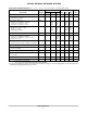
MC7800, MC7800A, MC7800AE, NCV7800 ORDERING INFORMATION Operating Temperature Range Package Shipping† MC7805BT TO-220 50 Units /Rail MC7805BTG TO-220 (Pb-free) 50 Units /Rail NCV7805BD2T* D2PAK 50 Units /Rail NCV7805BD2TG* D2PAK 50 Units /Rail Device Nominal Voltage (Pb-free) TJ = -40°C to +125°C NCV7805BD2TR4* NCV7805BD2TR4G* D2PAK 800 / Tape & Reel D2PAK 800 / Tape & Reel (Pb-free) NCV7805BT* TO-220 50 Units /Rail NCV7805BTG* TO-220 (Pb-free) 50 Units /Rail MC7805CD2T D2PAK
MC7800, MC7800A, MC7800AE, NCV7800 ORDERING INFORMATION Operating Temperature Range Package Shipping† MC7808ABD2T D2PAK 50 Units / Rail MC7808ABD2TG D2PAK 50 Units / Rail Device Nominal Voltage (Pb-free) MC7808ABD2TR4 TJ = -40°C to +125°C MC7808ABD2TR4G D2PAK 800 / Tape & Reel D2PAK 800 / Tape & Reel (Pb-free) MC7808ABT TO-220 50 Units / Rail MC7808ABTG TO-220 (Pb-free) 50 Units / Rail MC7808ACT TO-220 50 Units / Rail TO-220 (Pb-free) 50 Units / Rail TO-220 (Pb-free) 50 Units /
MC7800, MC7800A, MC7800AE, NCV7800 ORDERING INFORMATION Device Nominal Voltage Package Shipping† DPAK (Pb-free) 75 Units / Rail TO-220 (Pb-free) 50 Units / Rail TO-220 50 Units /Rail TJ = 0°C to +125°C TO-220 (Pb-free) 50 Units /Rail TO-220 50 Units /Rail TJ = -40°C to +125°C TO-220 (Pb-free) 50 Units /Rail D2PAK 50 Units /Rail D2PAK (Pb-free) 50 Units /Rail D2PAK 800 / Tape & Reel D2PAK 800 / Tape & Reel TJ = -40°C to +125°C NCV7808BDTG* NCV7808BTG* Operating Temperature Range
MC7800, MC7800A, MC7800AE, NCV7800 ORDERING INFORMATION Operating Temperature Range Package Shipping† MC7812BD2T D2PAK 50 Units /Rail MC7812BD2TG D2PAK 50 Units /Rail Device Nominal Voltage (Pb-free) MC7812BD2TR4 MC7812BD2TR4G 12 V TJ = -40°C to +125°C D2PAK 800 / Tape & Reel D2PAK 800 / Tape & Reel (Pb-free) MC7812BDT DPAK 75 Units / Rail DPAK (Pb-free) 75 Units / Rail DPAK 2500 / Tape & Reel DPAK (Pb-free) 2500 / Tape & Reel TO-220 50 Units / Rail TO-220 (Pb-free) 50 Units /
MC7800, MC7800A, MC7800AE, NCV7800 ORDERING INFORMATION Operating Temperature Range Package Shipping† MC7815ABD2T D2PAK 50 Units /Rail MC7815ABD2TG D2PAK 50 Units /Rail Device Nominal Voltage (Pb-free) MC7815ABD2TR4 TJ = -40°C to +125°C MC7815ABD2TR4G D2PAK 800 / Tape & Reel D2PAK 800 / Tape & Reel (Pb-free) MC7815ABT TO-220 50 Units /Rail MC7815ABTG TO-220 (Pb-free) 50 Units /Rail D2PAK 50 Units /Rail D2PAK 50 Units /Rail MC7815ACD2T 15 V MC7815ACD2TG (Pb-free) TJ = 0°C to +12
MC7800, MC7800A, MC7800AE, NCV7800 ORDERING INFORMATION Operating Temperature Range Package Shipping† MC7815CD2T D2PAK 50 Units /Rail MC7815CD2TG D2PAK 50 Units /Rail Device Nominal Voltage (Pb-free) MC7815CD2TR4 D2PAK 800 / Tape & Reel MC7815CD2TR4G D2PAK 800 / Tape & Reel (Pb-free) MC7815CDT DPAK 75 Units / Rail DPAK (Pb-free) 75 Units / Rail DPAK 2500 / Tape & Reel MC7815CDTRKG DPAK (Pb-free) 2500 / Tape & Reel MC7815CT TO-220 50 Units /Rail MC7815CTG TO-220 (Pb-free) 50 U
MC7800, MC7800A, MC7800AE, NCV7800 ORDERING INFORMATION Operating Temperature Range Package Shipping† TO-220 50 Units /Rail TO-220 (Pb-free) 50 Units /Rail MC7824BD2T D2PAK 50 Units /Rail MC7824BD2TG D2PAK 50 Units /Rail Device Nominal Voltage MC7824ACT TJ = 0°C to +125°C MC7824ACTG (Pb-free) MC7824BD2TR4 TJ = -40°C to +125°C MC7824BD2TR4G D2PAK 800 / Tape & Reel D2PAK 800 / Tape & Reel (Pb-free) MC7824BT TO-220 50 Units /Rail TO-220 (Pb-free) 50 Units /Rail D2PAK 50 Units /Rail
MC7800, MC7800A, MC7800AE, NCV7800 PACKAGE DIMENSIONS TO-220, SINGLE GAUGE T SUFFIX CASE 221AB-01 ISSUE O -TB SEATING PLANE C F T S 4 DIM A B C D F G H J K L N Q R S T U V Z A Q 1 2 3 U H K Z L R V NOTES: 1. DIMENSIONING AND TOLERANCING PER ANSI Y14.5M, 1982. 2. CONTROLLING DIMENSION: INCH. 3. DIMENSION Z DEFINES A ZONE WHERE ALL BODY AND LEAD IRREGULARITIES ARE ALLOWED. J G D N http://onsemi.com 31 INCHES MIN MAX 0.570 0.620 0.380 0.405 0.160 0.190 0.025 0.035 0.142 0.147 0.095 0.105 0.
MC7800, MC7800A, MC7800AE, NCV7800 PACKAGE DIMENSIONS D2PAK-3 D2T SUFFIX CASE 936-03 ISSUE B -TK OPTIONAL CHAMFER A TERMINAL 4 E U S B F V H 1 2 3 M J D 0.010 (0.254) M T NOTES: 1. DIMENSIONING AND TOLERANCING PER ANSI Y14.5M, 1982. 2. CONTROLLING DIMENSION: INCH. 3. TAB CONTOUR OPTIONAL WITHIN DIMENSIONS A AND K. 4. DIMENSIONS U AND V ESTABLISH A MINIMUM MOUNTING SURFACE FOR TERMINAL 4. 5. DIMENSIONS A AND B DO NOT INCLUDE MOLD FLASH OR GATE PROTRUSIONS.
MC7800, MC7800A, MC7800AE, NCV7800 PACKAGE DIMENSIONS DPAK-3 DT SUFFIX CASE 369C-01 ISSUE O -TC B V NOTES: 1. DIMENSIONING AND TOLERANCING PER ANSI Y14.5M, 1982. 2. CONTROLLING DIMENSION: INCH. SEATING PLANE E R 4 Z A S 1 2 DIM A B C D E F G H J K L R S U V Z 3 U K F J L H D G 2 PL 0.13 (0.005) M INCHES MIN MAX 0.235 0.245 0.250 0.265 0.086 0.094 0.027 0.035 0.018 0.023 0.037 0.045 0.180 BSC 0.034 0.040 0.018 0.023 0.102 0.114 0.090 BSC 0.180 0.215 0.025 0.040 0.020 --0.035 0.050 0.