
Datasheet


MC7800, MC7800A, MC7800AE, NCV7800
http://onsemi.com
10
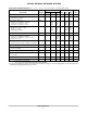
ELECTRICAL CHARACTERISTICS (V
in
= 15 V, I
O
= 1.0 A, T
J
= 0°C to 125°C, unless otherwise noted)
Characteristic Symbol
MC7809AC
Unit
Min Typ Max
Output Voltage (TJ = 25°C) VO 8.82 9.0 9.18 Vdc
Output Voltage (5.0 mA ≤ IO ≤ 1.0 A, PD ≤ 15 W)
11.5 Vdc ≤ Vin ≤ 24 Vdc
VO 8.65 9.0 9.35 Vdc
Line Regulation (Note 15)
11.5 Vdc ≤ Vin ≤ 26 Vdc, IO = 500 mA
12 Vdc ≤ Vin ≤ 17 Vdc, IO = 1.0 A
11.5 Vdc ≤ Vin ≤ 24 Vdc, TJ = 25°C
Regline
-
-
-
6.2
1.8
5.2
16
7.0
16
mV
Load Regulation (Note 15)
5.0 mA ≤ IO ≤ 1.5 A, TJ = 25°C
5.0 mA ≤ IO ≤ 1.0 A
250 mA ≤ IO ≤ 750 mA
Regload
-
-
-
-
-
-
25
25
15
mV
Quiescent Current IB - 3.3 6.0 mA
Quiescent Current Change
11.5 Vdc ≤ Vin ≤ 26 Vdc, IO = 500 mA
11.5 Vdc ≤ Vin ≤ 24 Vdc, IO = 1.0 A, TJ = 25°C
5.0 mA ≤ IO ≤ 1.0 A
DIB
-
-
-
-
-
-
0.8
0.8
0.5
mA
Ripple Rejection
11.5 Vdc ≤ Vin ≤ 21.5 Vdc, f = 120 Hz, IO = 500 mA
RR
56 61 -
dB
Dropout Voltage (IO = 1.0 A, TJ = 25°C) VI _ VO 2.0 Vdc
Output Noise Voltage (TA = 25°C)
10 Hz ≤ f ≤ 100 kHz
Vn
- 10 -
mV/VO
Output Resistance f = 1.0 kHz rO - 1.0 -
mW
Short Circuit Current Limit (TA = 25°C)
Vin = 35 Vdc
ISC - 0.2 A
Peak Output Current (TJ = 25°C) Imax - 2.2 - A
Average Temperature Coefficient of Output Voltage TCVO - -0.5 - mV/°C
15.Load and line regulation are specified at constant junction temperature. Changes in VO due to heating effects must be taken into account
separately. Pulse testing with low duty cycle is used.