
Datasheet


NCP1010, NCP1011, NCP1012, NCP1013, NCP1014
http://onsemi.com
3
PIN FUNCTION DESCRIPTION
Pin No.
(SOT--223)
Pin No.
(PDIP--7,
PDIP--7/Gull Wing)
Pin Name Function Description
1 1 V
CC
Powers the Internal Circuitry This pin is connected to an external capacitor of typic-
ally 10 mF. The natural ripple superimposed on the
V
CC
participates to the frequency jittering. For im-
proved standby performance, an auxiliary V
CC
can be
connected to Pin 1. The V
CC
also includes an active
shunt which serves as an opto fail--safe protection.
-- 2 NC -- --
-- 3 GND The IC Ground --
2 4 FB Feedback Signal Input By connecting an optocoupler to this pin, the peak
current setpoint is adjusted accordingly to the output
power demand.
3 5 Drain Drain Connection The internal drain MOSFET connection.
-- -- -- -- --
-- 7 GND The IC Ground --
4 8 GND The IC Ground --
65, 100 or
130 kHz
Clock
Overload?
UVLO
Management
GND
NC
V
CC
FB
Drain
GND
GND
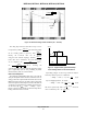
Figure 2. Simplified Internal Circuit Architecture
2
1
3
4
IV
CC
I?
Vclamp*
4V
18 k
Error flag a rmed?
EMI Jittering
V
CC
Startup S ource
Drain
Flip--Flop
DCmax = 65%
Reset
Reset
High when V
CC
< 3V
Driver
S
Q
R
--
+
Iref = 7.4 mA
IV
CC
Set
Q
V
CC
8
Rsense
250 ns
L.E.B.
7
5
--
+
+
--
Soft--Start
Startup S equence
Overload
--
+
0.5 V
Drain
*Vclamp = VCC
OFF
+ 200 mV (8.7 V Typical)