
Datasheet


NCP1010, NCP1011, NCP1012, NCP1013, NCP1014
http://onsemi.com
5
ELECTRICAL CHARACTERISTICS (For typical values T
J
=25C, for min/max values T
J
=--40C to +125C, Max T
J
= 150C,
V
CC
= 8.0 V unless otherwise noted.)
Rating
Pin Symbol Min Typ Max Unit
SUPPLY SECTION AND V
CC
MANAGEMENT
V
CC
Increasing Level at which the Current Source Turns--off 1 VCC
OFF
7.9 8.5 9.1 V
V
CC
Decreasing Level at which the Current Source Turns-- on 1 VCC
ON
6.9 7.5 8.1 V
Hysteresis between VCC
OFF
and VCC
ON
1 -- -- 1.0 -- V
V
CC
Decreasing Level at which the Latch--off Phase Ends 1 VCC
latch
4.4 4.7 5.1 V
V
CC
Decreasing Level at which the Internal Latch is Released 1 VCC
reset
-- 3.0 -- V
Internal IC Consumption, MOSFET Switching at 65 kHz (Note 2) 1 ICC1 -- 0.92 1.1 mA
Internal IC Consumption, MOSFET Switching at 100 kHz (Note 2) 1 ICC1 -- 0.95 1.15 mA
Internal IC Consumption, MOSFET Switching at 130 kHz (Note 2) 1 ICC1 -- 0.98 1.2 mA
Internal IC Consumption, Latch--off Phase, V
CC
=6.0V 1 ICC2 -- 290 --
mA
Active Zener Voltage Positive Offset to VCC
OFF
1 Vclamp 140 200 300 mV
Latch--off Current
NCP1012/13/14 0C<T
J
< 125C
-- 4 0 C<T
J
< 125C
NCP1010/11 0C<T
J
< 125C
-- 4 0 C<T
J
< 125C
1 ILatch
6.3
5.8
5.8
5.3
7.4
7.4
7.3
7.3
9.2
9.2
9.0
9.0
mA
POWER SWITCH CIRCUIT
Power Switch Circuit On--state Resistance
NCP1012/13/14 (Id = 50 mA)
T
J
=25C
T
J
= 125C
NCP1010/11 (Id = 50 mA)
T
J
=25C
T
J
= 125C
5 R
DSon
--
11
19
22
38
16
24
35
50
Ω
Power S witch Circuit and Startup Breakdown Voltage
(ID
(off)
= 120 mA, T
J
=25C)
5 BVdss 700 -- -- V
Power Switch and Startup Breakdown Voltage Off--state Leakage Current
T
J
=--40C (Vds = 650 V)
T
J
=25C (Vds = 700 V)
T
J
= 125C (Vds = 700 V)
5
5
5
I
DS(OFF
)
--
--
--
70
50
30
120
--
--
mA
Switching Characteristics (RL = 50 Ω, Vds Set for Idrain = 0.7 x Ilim)
Turn--on Time (90%--10%)
Turn--off Time (10%--90%)
5
5
ton
toff
--
--
20
10
--
--
ns
INTERNAL STARTUP CURRENT SOURCE
High--voltage Current Source, V
CC
=8.0V
NCP1012/13/14 0C<T
J
< 125C
-- 4 0 C<T
J
< 125C
NCP1010/11 0C<T
J
< 125C
-- 4 0 C<T
J
< 125C
1 IC1
5.0
5.0
5.0
5.0
8.0
8.0
8.0
8.0
10
11
10.3
11.5
mA
High--voltage Current Source, V
CC
=0 1 IC2 -- 10 -- mA
CURRENT COMPARATOR T
J
=25C(Note2)
Maximum Internal Current Setpoint, NCP1010 (Note 3)
5 Ipeak (22) 90 100 110 mA
Maximum Internal Current Setpoint, NCP1011 (Note 3) 5 Ipeak (22) 225 250 275 mA
Maximum Internal Current Setpoint, NCP1012 (Note 3) 5 Ipeak (11) 225 250 275 mA
Maximum Internal Current Setpoint, NCP1013 (Note 3) 5 Ipeak (11) 315 350 385 mA
Maximum Internal Current Setpoint, NCP1014 (Note 3) 5 Ipeak (11) 405 450 495 mA
Default Internal Current Setpoint for Skip--Cycle Operation, Percentage of
Max Ip
-- I
Lskip
-- 25 -- %
Propagation Delay from Current Detection to Drain OFF State -- T
DEL
-- 125 -- ns
Leading Edge Blanking Duration -- T
LEB
-- 250 -- ns
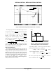
2. See characterization curves for temperature evolution.
3. Adjust di/dt to reach Ipeak in 3.2 msec.