NCP3063, NCP3063B, NCV3063 1.5 A, Step-Up/Down/ Inverting Switching Regulators http://onsemi.com The NCP3063 Series is a higher frequency upgrade to the popular MC34063A and MC33063A monolithic DC−DC converters. These devices consist of an internal temperature compensated reference, comparator, a controlled duty cycle oscillator with an active current limit circuit, a driver and a high current output switch.
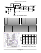
NCP3063, NCP3063B, NCV3063 1 Switch Collector Switch Emitter 2 8 N.C. 7 Ipk Sense Timing Capacitor 3 6 GND 4 5 ÇÇ ÇÇ ÇÇ ÇÇ Switch Collector Switch Emitter Timing Capacitor VCC GND Comparator Inverting Input (Top View) EP Flag Ç Ç Ç Ç (Top View) NOTE: Figure 2. Pin Connections N.C. Ipk Sense VCC Comparator Inverting Input EP Flag must be tied to GND Pin 4 on PCB Figure 3. Pin Connections NCP3063 8 1 TSD N.C.
NCP3063, NCP3063B, NCV3063 PIN DESCRIPTION Pin No. Pin Name Description 1 Switch Collector 2 Switch Emitter 3 Timing Capacitor Oscillator Input 4 GND 5 Comparator Inverting Input 6 VCC 7 Ipk Sense 8 N.C.
NCP3063, NCP3063B, NCV3063 ELECTRICAL CHARACTERISTICS (VCC = 5.0 V, TJ = Tlow to Thigh [Note 5], unless otherwise specified) Characteristic Conditions Min Typ Max Unit Frequency (VPin 5 = 0 V, CT = 2.2 nF, TJ = 25°C) 110 150 190 kHz IDISCHG / ICHG Discharge to Charge Current Ratio (Pin 7 to VCC, TJ = 25°C) 5.5 6.0 6.
NCP3063, NCP3063B, NCV3063 450 190 400 180 FREQUENCY (kHz) FREQUENCY (kHz) 350 300 250 200 150 100 170 160 150 140 130 120 50 0 110 0 1 2 3 4 5 6 7 8 9 10 11 12 1314 1516 1718 1920 7 12 16 21 25 29 34 38 40 VCC, SUPPLY VOLTAGE (V) Figure 5. Oscillator Frequency vs. Oscillator Timing Capacitor Figure 6. Oscillator Frequency vs. Supply Voltage 1.25 VCC = 5.0 V IE = 1 A VCC = 5.0 V IC = 1 A 1.20 VOLTAGE DROP (V) 2.2 VOLTAGE DROP (V) 3 Ct, CAPACITANCE (nF) 2.4 2.0 1.8 1.6 1.4 1.
Vth, COMPARATOR THRESHOLD VOLTAGE (V) NCP3063, NCP3063B, NCV3063 0.30 Vipk(sense), CURRENT LIMIT SENSE VOLTAGE (V) 1.30 1.28 1.26 1.24 1.22 1.20 −40 −25 −10 5 20 35 50 65 80 95 110 125 0.28 0.26 0.24 0.22 0.20 0.18 0.16 0.14 0.12 0.10 −40 −25 −10 TJ, JUNCTION TEMPERATURE (°C) 5 20 ICC, SUPPLY CURRENT (mA) 5.5 5.0 4.5 4.0 3.5 CT = 2.2 nF Pin 5, 7 = VCC Pin 2 = GND 3.0 2.5 8.0 65 80 95 110 125 Figure 12. Current Limit Sense Voltage vs. Temperature 6.0 3.
NCP3063, NCP3063B, NCV3063 INTRODUCTION The NCP3063 is a monolithic power switching regulator optimized for dc to dc converter applications. The combination of its features enables the system designer to directly implement step−up, step−down, and voltage− inverting converters with a minimum number of external components. Potential applications include cost sensitive consumer products as well as equipment for industrial markets. A representative block diagram is shown in Figure 4.
NCP3063, NCP3063B, NCV3063 Peak Current Sense Comparator Real Vturn−off on Rsc resistor With a voltage ripple gated converter operating under normal conditions, output switch conduction is initiated by the Voltage Feedback comparator and terminated by the oscillator. Abnormal operating conditions occur when the converter output is overloaded or when feedback voltage sensing is lost. Under these conditions, the Ipk Current Sense comparator will protect the Darlington output Switch.
NCP3063, NCP3063B, NCV3063 (See Notes 9, 10, 11) ton toff Step−Down Step−Up Voltage−Inverting Vout ) VF Vin * VSWCE * Vout Vout ) VF * Vin Vin * VSWCE |Vout| ) VF Vin * VSWCE ton toff ton toff ton ton toff f ǒton ) 1Ǔ f ǒton ) 1Ǔ t f ǒton ) 1Ǔ t off t off CT 10 *6 CT + 381.6 @ fosc off * 343 @ 10 *12 ǒ Ǔ ǒ Ǔ IL(avg) Iout t Iout on ) 1 toff t Iout on ) 1 toff Ipk (Switch) DI IL(avg) ) L 2 DI IL(avg) ) L 2 DI IL(avg) ) L 2 RSC 0.20 Ipk (Switch) 0.20 Ipk (Switch) 0.
NCP3063, NCP3063B, NCV3063 U201 8 N.C. SWC 7 SWE IPK 6 VCC TCAP 5 COMP GND R201 0R15 +VIN = +12 V 1 J201 C201 0.1 mF + C202 220 mF / 50 V 1 2 L201 +VOUT = +3.3 V / 800 mA 47 mH 1 3 4 C203 2.2 nF NCP3063 C206 D201 1N5819 0.1 mF J203 + C205 470 mF / 25 V 1 J202 GND R203 1 GND J204 3K9 ±1% R202 2K4 ±1% Figure 16. Typical Buck Application Schematic Value of Components Name Value Name Value L201 47 mH, Isat > 1.5 A R201 150 mW, 0.
NCP3063, NCP3063B, NCV3063 L101 R101 0R15 +VIN = +12 V 8 7 6 5 1 J101 C101 0.1 mF + C102 470 mF / 25 V 100 mH U101 N.C. SWC 1 SWE 2 IPK 3 VCC TCAP COMP GND 4 D101 C106 C103 0.1 mF 2.2 nF NCP3063 +VOUT = +24 V / 350 mA 1N5819 1 J103 + C105 330 mF / 50 V J104 1 J102 GND R103 1 GND R102 1K0 ±1% 18K0 ±1% Figure 19. Typical Boost Application Schematic Value of Components Name Value Name Value L101 100 mH, Isat > 1.5 A R101 150 mW, 0.5 W D101 1 A, 40 V Schottky Rectifier R102 1.
NCP3063, NCP3063B, NCV3063 U501 8 N.C. SWC 7 SWE IPK 6 VCC TCAP 5 COMP GND R501 0R15 +VIN = +5 V 1 J501 C501 0.1 mF + 1 2 3 4 NCP3063 C502 330 mF / 25 V J502 C503 L501 2.2 nF 22 mH D501 1N5819 VOUT = −12 V / 100 mA R503 1 1 J503 C506 1K96 ±1% GND R502 16K9 ±1% C505 + 470 mF / 35 V 0.1 mF 1 J504 GND Figure 22. Typical Voltage Inverting Application Schematic Value of Components Name Value Name Value L501 22 mH, Isat > 1.5 A R501 150 mW, 0.
NCP3063, NCP3063B, NCV3063 VIN = 8 − 18 V/0.6 A R1 82m R2 1k L1 C5 IC1 NCP3063 8 N.C. SWC 1 7 SWE 2 IPK 6 TC 3 VCC 5 COMP GND 4 C3 C1 C2 R3 M18 330m 100n Q1 NTD18N06 D 6n8 R7 6 1G 470 2 4 5 3 D1 S IC2 BC846BPD 10n R5 1N5819 VOUT = 31 V/0.35 A 10m 24k C4 R4 1k R8 1k 1n2 C6 C7 + 100n 330m 0V GND Figure 25.
NCP3063, NCP3063B, NCV3063 VIN = 8 − 19 V R1 Q2 NTGS4111P 50m T1 6 BC848CPD 2 R5 1k IC1 NCP3063 8 N.C. SWC 1 7 SWE 2 IPK 6 TC 3 VCC 5 COMP GND 4 R2 C1 + 330m C2 3 5 1 4 R6 22k 1k7 C5 R3 1k 100n VOUT = 3V3/3 A 10m L1 2n2 R8 470 C4 6n8 D1 1N5822 C6 100n 0V C7 + 330m GND Figure 27. Typical Buck Application Schematic with External PMOS Transistor Figure 27 shows typical buck configuration with external PMOS transistor.
NCP3063, NCP3063B, NCV3063 R1 VIN = 8 − 19 V Q1 L1 NSS35200 150m D2 R4 33 NSR0130 IC1 NCP3063 8 N.C. SWC 1 7 SWE 2 IPK 6 TC 3 VCC 5 COMP GND 4 R3 C1 + C2 100m 100n VOUT = 3V3/1 A 33m R5 33 1k7 C3 R2 1k 2n2 D1 1N5819 C5 100n C6 + 100m 0V GND Figure 29. Typical Buck Application Schematic with External Low VCE(sat) PNP Transistor 100 Typical application of the buck converter with external bipolar transistor is shown in the Figure 29.
NCP3063, NCP3063B, NCV3063 R1 IC1 NCP3063 8 N.C. SWC 7 SWE IPK 6 TC VCC 5 COMP GND 1 2 3 L1 4 R5 22k R2 C1 10R C2 R3 R4 C3 C4 D1 4n7 0V 0V Figure 31. Typical Schematic of Buck Converter with RC Snubber and Pulse Feedback In some cases where there are oscillations on the output due to the input/output combination, output load variations or PCB layout a snubber circuit on the SWE Pin will help minimize the oscillation. Typical usage is shown in the Figure 31.
NCP3063, NCP3063B, NCV3063 PACKAGE DIMENSIONS SOIC−8 NB CASE 751−07 ISSUE AJ −X− NOTES: 1. DIMENSIONING AND TOLERANCING PER ANSI Y14.5M, 1982. 2. CONTROLLING DIMENSION: MILLIMETER. 3. DIMENSION A AND B DO NOT INCLUDE MOLD PROTRUSION. 4. MAXIMUM MOLD PROTRUSION 0.15 (0.006) PER SIDE. 5. DIMENSION D DOES NOT INCLUDE DAMBAR PROTRUSION. ALLOWABLE DAMBAR PROTRUSION SHALL BE 0.127 (0.005) TOTAL IN EXCESS OF THE D DIMENSION AT MAXIMUM MATERIAL CONDITION. 6. 751−01 THRU 751−06 ARE OBSOLETE. NEW STANDARD IS 751−07.
NCP3063, NCP3063B, NCV3063 PACKAGE DIMENSIONS 8 LEAD PDIP CASE 626−05 ISSUE L 8 5 −B− 1 4 F −A− NOTE 2 L C J −T− N SEATING PLANE D H NOTES: 1. DIMENSION L TO CENTER OF LEAD WHEN FORMED PARALLEL. 2. PACKAGE CONTOUR OPTIONAL (ROUND OR SQUARE CORNERS). 3. DIMENSIONING AND TOLERANCING PER ANSI Y14.5M, 1982. M K G 0.13 (0.005) M T A M B M http://onsemi.com 18 DIM A B C D F G H J K L M N MILLIMETERS MIN MAX 9.40 10.16 6.10 6.60 3.94 4.45 0.38 0.51 1.02 1.78 2.54 BSC 0.76 1.27 0.20 0.30 2.
NCP3063, NCP3063B, NCV3063 PACKAGE DIMENSIONS 8 PIN DFN, 4x4 CASE 488AF−01 ISSUE C A B D PIN ONE REFERENCE 2X 0.15 C 2X 0.10 C 8X 0.08 C DETAIL A E OPTIONAL CONSTRUCTIONS EXPOSED Cu ÇÇÇÇ DETAIL B (A3) A A1 C ÇÇÇ ÇÇ ÇÇÇ ÇÇ ÇÇÇÇ 8 e MOLD CMPD A1 ALTERNATE CONSTRUCTIONS SEATING PLANE L 8X MILLIMETERS MIN MAX 0.80 1.00 0.00 0.05 0.20 REF 0.25 0.35 4.00 BSC 1.91 2.21 4.00 BSC 2.09 2.39 0.80 BSC 0.20 −−− 0.30 0.50 −−− 0.15 2.