
Datasheet


NCP3063, NCP3063B, NCV3063
http://onsemi.com
2
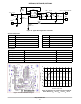
Figure 2. Pin Connections
Timing Capacitor
Comparator
Inverting
Input
V
CC
N.C.
I
pk
Sense
GND
Switch Emitter
Switch Collector
(Top View)
4
3
2
1
5
6
7
8
Ç
Ç
Ç
Ç
ÇÇ
ÇÇ
ÇÇ
ÇÇ
Comparator
Inverting
Input
V
CC
N.C.
I
pk
Sense
Timing Capacitor
GND
Switch Emitter
Switch Collector
(Top View)
Figure 3. Pin Connections
NOTE: EP Flag must be tied to GND Pin 4
on PCB
EP Flag
Figure 4. Block Diagram
REFERENCE
COMPARATOR
5
R
S
Q
SET dominant
+
−
7
COMPARATOR
CT
3
1.25 V
8
NCP3063
REGULATOR
TSD
0.2 V
+
−
2
6
R
S
Q
4
1
OSCILLATOR
Switch Collector
Switch Emitter
Timing Capacitor
GND
Comparator Inverting Input
+V
CC
I
pk
Sense
N.C.
SET dominant