
Datasheet


NCP3063, NCP3063B, NCV3063
http://onsemi.com
8
Peak Current Sense Comparator
With a voltage ripple gated converter operating under
normal conditions, output switch conduction is initiated by
the Voltage Feedback comparator and terminated by the
oscillator. Abnormal operating conditions occur when the
converter output is overloaded or when feedback voltage
sensing is lost. Under these conditions, the I
pk
Current Sense
comparator will protect the Darlington output Switch. The
switch current is converted to a voltage by inserting a
fractional ohm resistor, R
SC
, in series with V
CC
and the
Darlington output switch. The voltage drop across R
SC
is
monitored by the Current Sense comparator. If the voltage
drop exceeds 200 mV with respect to V
CC
, the comparator
will set the latch and terminate output switch conduction on
a cycle−by−cycle basis. This Comparator/Latch
configuration ensures that the Output Switch has only a
single on−time during a given oscillator cycle.
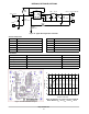
Real
V
turn−off
on
R
s
Resistor
t_delay
I1
Io
di/dt slope
I through the
Darlington
Switch
V
ipk(sense)
The V
IPK(Sense)
Current Limit Sense Voltage threshold is
specified at static conditions. In dynamic operation the
sensed current turn−off value depends on comparator
response time and di/dt current slope.
Real V
turn−off
on R
sc
resistor
V
turn_off
+ V
ipk(sense)
) Rs @ (t_delay @ dińdt)
Typical I
pk
comparator response time t_delay is 350 ns.
The di/dt current slope is growing with voltage difference on
the inductor pins and with decreasing inductor value.
It is recommended to check the real max peak current in
the application at worst conditions to be sure that the max
peak current will never get over the 1.5 A Darlington Switch
Current max rating.
Thermal Shutdown
Internal thermal shutdown circuitry is provided to protect
the IC in the event that the maximum junction temperature
is exceeded. When activated, typically at 160°C, the Output
Switch is disabled. The temperature sensing circuit is
designed with 10°C hysteresis. The Switch is enabled again
when the chip temperature decreases to at least 150°C
threshold. This feature is provided to prevent
catastrophic failures from accidental device
overheating. It is not intended to be used as a
replacement for proper heatsinking.
Output Switch
The output switch is designed in a Darlington
configuration. This allows the application designer to
operate at all conditions at high switching speed and low
voltage drop. The Darlington Output Switch is designed to
switch a maximum of 40 V collector to emitter voltage and
current up to 1.5 A.
APPLICATIONS
Figures 16 through 24 show the simplicity and flexibility
of the NCP3063. Three main converter topologies are
demonstrated with actual test data shown below each of the
circuit diagrams.
Figure 15 gives the relevant design equations for the key
parameters. Additionally, a complete application design aid
for the NCP3063 can be found at www.onsemi.com.
Figures 25 through 31 show typical NCP3063
applications with external transistors. This solution helps to
increase output current and helps with efficiency still
keeping low cost bill of materials. Typical schematics of
boost configuration with NMOS transistor, buck
configuration with PMOS transistor and buck configuration
with LOW V
CE(sat)
PNP are shown.
Another advantage of using the external transistor is
higher operating frequency which can go up to 250 kHz.
Smaller size of the output components such as inductor and
capacitor can be used then.